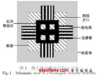
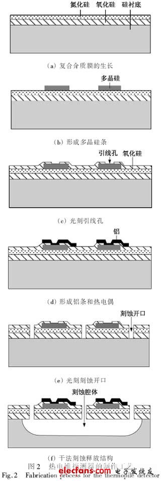
In this paper, a thermoelectric stack structure with a front opening is realized, and XeF2 is used as a working gas dry etching process to release the device. Compared to etched silicon, XeF2 gas has a very low etch rate for materials such as aluminum, so that the most commonly used materials in standard CMOS processes, such as Poly/Al, can be used to form thermocouples, which greatly improves compatibility. 1 Design and production The thermopile detector proposed in this paper comprises a silicon substrate, a frame, a thermopile, a support arm, an infrared absorption layer, and an etching opening. The six parts are shown in Fig. 1, wherein the substrate and the infrared absorption layer suspended in the middle of the frame respectively constitute a thermoelectricity. The cold junction zone and the hot junction zone of the stack, the support arm serves as a connection frame and an infrared absorption zone and carries the thermopile. The support arm and the infrared absorbing layer are composed of a composite film of silicon oxide and silicon nitride deposited on single crystal silicon. A particular feature of the structure is the fabrication of an intermediate suspended infrared absorbing layer and the design of an etched opening for dry etching the substrate. Due to the isotropy of the dry etching, the shape of the etching opening can be varied, and the wet etching opening must be arranged strictly along a specific crystal direction, thereby greatly increasing the design flexibility. The thermopile infrared detector is processed based on MEMS technology. The process steps are shown in Figure 2, Figure 2 (a) The growth of the composite dielectric film. On the polished Si wafer, silicon oxide is first thermally grown by 0.5 to 0.6 μm, and then SiN is deposited by LPCVD to a thickness of 0.1 to 0.2 μm to form a silicon oxide-silicon nitride composite dielectric film structure. (b) forming a polysilicon strip. Polycrystalline silicon (0.8-1.0 μm) was deposited by LPCVD on the composite dielectric film, and B ion implantation was doped, and the sheet resistance was annealed to 30 to 40 Ω. The first photolithography, BOE etching or ion beam etching forms a polysilicon strip as a component of the thermocouple. (c) Photolithographic lead holes. On the polysilicon formed in (b), a layer of silicon oxide (0.5 to 0.6 μm) is deposited as an insulating layer, and a second photolithography is performed to form a lead hole. (d) Forming aluminum strips and thermocouples. Sputtering Al, a third photolithography, and wet etching form an aluminum strip to form a thermocouple. (e) Photolithographic etching of the opening. The fourth photolithography forms a gas channel for dry etching. (f) Dry etching release structure. The working gas etches the silicon substrate via the etch opening formed in (e) to form a suspended absorber layer, releasing the thermopile structure. Figure 3 shows the fabricated thermopile device. RAM/RFM Induction Heating Capacitors
RAM/RFM induction heating capacitors
RAM/RFM Induction Heating Capacitors,Water Pump Capacitor,Water Cooled Condense,Tank Capacitor,RAM/RFM Induction Heating Capacitors YANGZHOU POSITIONING TECH CO., LTD. , https://www.cndingweitech.com