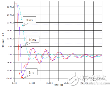
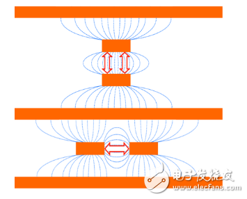
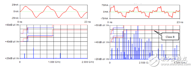
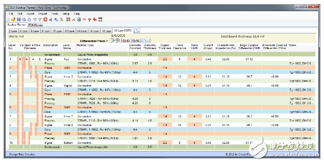
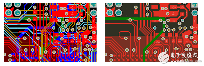
In the field of electronic design, high performance design has its own unique challenges. The birth of high-speed design In recent years, the increasing number of high frequency signal designs has been closely linked to the steadily increasing performance of electronic systems. As system performance improves, PCB designers are increasingly challenged: smaller die sizes, denser board layouts, and lower power chip requirements. With the rapid development of all technologies, we have become the core of high-speed design, considering its complexity and all factors. review In the past 30 years, PCB design has changed a lot. In 1987, we thought that 0.5 micron was the terminator of technology, but today, the 22 nanometer process has become the norm. As shown in the following figure, the edge rate in 1985 advanced the design complexity (usually 30 nanoseconds), and today the edge rate has become 1 nanosecond. Changes in edge rate over the past 30 years Various problems accompanying technological progress Advances in technology are always accompanied by a series of problems. As system performance improves and high-speed design is adopted, some issues must be addressed in the design environment. Below, let's summarize the challenges we face: Signal quality IC manufacturers tend to have lower core voltages and higher operating frequencies, which leads to sharply rising edge rates. Edge rates in unterminated designs can cause reflection and signal quality problems. Crosstalk In high-speed signal design, dense paths tend to cause crosstalk—the electromagnetic coupling between the traces on the PCB. Crosstalk can be either edge coupling of traces on the same layer or wide edge coupling on adjacent layers. The coupling is three-dimensional. Parallel paths and wide-edge traces cause more crosstalk than side-by-side trace paths. Wide-edge coupling (top) compared to edge coupling (bottom) radiation The fast edge rate in traditional designs, even with the same frequency and trace length as before, produces ringing on the unterminated transmission line. This fundamentally leads to higher emissions, far exceeding the FCC/CISPR Class B limits for terminalless transmission lines. Edge rate radiation of 10 nanoseconds (left) and 1 nanosecond (right) Design solution Signal and power integrity issues occur intermittently and are difficult to discriminate. So the best way is to find the root cause of the problem in the design process, and clear it, instead of trying to solve it in the later stage, delay production. The Laminated Planning tool makes it easier to implement solutions to signal integrity problems in your design. Board stack planning The first big thing in high-speed design must be the board stack. The substrate is the most important component of the assembly and its specifications must be carefully planned to avoid discontinuous impedance, signal coupling and excessive electromagnetic radiation. Keep the following tips and suggestions in mind when looking at the board stack you are designing next time: All signal layers need to be adjacent and tightly coupled to an uninterrupted reference plane that creates a clear loop that eliminates wide-edge crosstalk. The substrate of each signal layer is adjacent to the reference plane There is good planar capacitance to reduce the AC impedance at high frequencies. The tightly coupled inner plane plane reduces the AC impedance of the top layer and greatly reduces electromagnetic radiation. Reducing the dielectric height greatly reduces crosstalk without affecting the available space on the board. The substrate should be adaptable to a range of different technologies. For example: 50/100 ohm digits, 40/80 ohm DDR4, 90 ohm USB. Wiring and workflow After carefully planning the stack, the next step is to pay attention to the board layout. Based on design rules and careful configuration of your work area, you can route your board most efficiently and successfully. These tips can help you make wiring easier and avoid unnecessary crosstalk, radiation, and signal quality issues: Simplify the view to clearly see the split plane and current loop. To do this, first determine which copper foil plane (ground or power) is used as the reference plane for each signal layer, then open the signal layer and the inner layer plane simultaneously. This will help you more easily see the traces of the split plane. Multiple signal layers (left), top layer, and adjacent plan views (right) If the digital signal must cross the power reference plane, you can place one or two decoupling capacitors (100nF) close to the signal. This provides a current loop between the two power supplies. Avoid parallel and wide-edge routing, which can cause more crosstalk than side-by-side routing. Unless a synchronous bus is used, the shorter the parallel interval, the better, to reduce crosstalk. Leave space for the signal group so that its address and data interval is three times the width of the trace. Be careful when using the combined microstrip layer on the top and bottom layers of the board. This can lead to crosstalk between adjacent layers, jeopardizing signal integrity. The clock (or strobe) signal is routed according to the longest delay of the signal group, which ensures that the data has been established before the clock is read. Interleaving the embedded signal between planes helps minimize radiation and provides ESD protection. Signal clarity In the future, the complexity of electronic design will undoubtedly continue to increase, which will bring a series of challenges to PCB designers. Ensuring proper stacking of boards, impedance, and current loops is the basis for design stability. Timer,Electronic Timer, Waterproof Timer, Countdown Timer NINGBO COWELL ELECTRONICS & TECHNOLOGY CO., LTD , https://www.cowellsocket.com