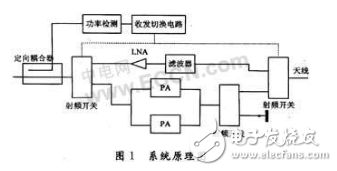
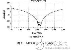
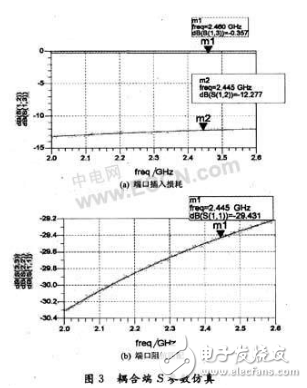
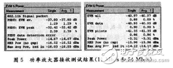
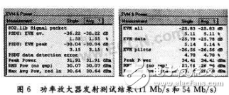
In the WLAN network, since the low power and high frequency of the WLAN limit its coverage, the existing products basically have a relatively small communication distance, and relatively few two-way transmission and reception are realized. At present, many power amplifiers are integrated in the transceiver, which improves the integration and simplifies the circuit. However, the power of the integrated power amplifier is often not large enough, and it is necessary to add a power module for long-distance transmission. This paper mainly studies the design and hardware implementation of wireless power amplifier, which is realized by increasing the transmit signal power and amplifying the received signal to improve the sensitivity. At the same time, the bidirectional transmission and reception of signals can be realized, which can be applied to the long distance of 802.11b/g mode. Wireless transmission. As shown in FIG. 1 , in the system schematic diagram, a part of the power input to the RF input channel is sent to the detection circuit for processing, and the detected RF envelope and the fixed threshold level are compared to control the transmission and reception status of the signal port, if higher than the gate. Limit the level, switch the RF switch, have a signal to transmit, open the transmit channel, and vice versa. 1.1 Transmission microstrip line design The microstrip line is the focus of the RF circuit design, is part of the module matching network, and is also a bridge connecting the various functional modules. The transmission microstrip line is used for the input/output signal or the connection circuit. If it matches the output impedance of the front end circuit and the input impedance of the back end circuit, the power loss during signal transmission can be reduced to the transmission micro in the most school-based design. The line characteristic impedance is 50Ω. The characteristic impedance value of the microstrip line is determined by parameters such as the width w of the microstrip line, the dielectric constant ε of the PCB board, the large thickness H of the PCB board, and the thickness T of the copper foil. Under certain conditions of the material, the characteristic impedance depends only on the width w of the microstrip line. FR4 sheet is used in this design. From equation (1): The function of the transmission power amplifying circuit is to amplify the transmission signal and output a large power. In this circuit, a double-tube balanced amplifying circuit is adopted, and a parallel method is adopted to increase the output power. The power amplifier chip selects anadigics' AWL6153UM7P8, which can achieve 25dBm at 54Mb/s signal rate at 5V DC voltage and 802.11g mode. The two identical application circuits of the chip are connected in parallel to form a balanced amplifier circuit to increase the output power. In Figure 2, in the software Agilent ADS2004 environment, the results of the parameter S simulation can be seen that the port insertion loss is less than 3dB at 2.4GHz, and the output power of the amplifier circuit can reach 27dBm, which is 500mW. 1.3 Low noise amplification receiver circuit design The low noise amplification receiving circuit improves the sensitivity of the received signal. The design circuit selects the RFMD2373 chip, which can provide a maximum gain of 15dB and a low noise figure of 1.3dB and consumes only 10mA. The first-order gain compression point (P1dB)-3.5dBm at 2.4GHz, the third-order intersection intercept point (IP3) It is 9.5dBm. Adding a band-pass filter to the input can effectively filter out noise. 1.4 detection circuit design In order not to make the power detector output a large voltage value when the receiving power is large, and to prevent the power detecting circuit from affecting the characteristic impedance of the circuit, the power detector input terminal uses a directional coupler to couple a part of the power input from the path to the detecting circuit. The switching control signal is obtained by shaping and transforming the output signal of the power detecting circuit. In the circuit, a part of the energy is coupled from the RF main path to the chip to detect the transmitted signal. The main channel attenuation is less than 1dB, and the coupling degree is 13dB. The S parameter simulation under ADS software is shown in Figure 3. The physical dimensions of the microstrip coupling line are: microstrip line width w=11.8 mil, spacing s=3.9 mil, coupling line length L=531 mil. 1.5 switch switching control circuit and power circuit design The signal outputted by the detection circuit cannot directly control the RF signal, and the triode MBT2222 is used as a driving circuit to control the RF switch to realize the transmission and reception switching of the power amplifier. The power circuit converts the 9V voltage to 5V to provide the normal operating voltage of the power module. 2.1 Port S parameter test The power amplifier port S parameter test uses the Agilient E5071B vector network analyzer, and the test results are shown in Figure 4. 2.2 Communication test The IQVIEW test instrument emits a -30dBm RF signal as the power amplifier input signal to test the reception performance. In the software IQsignalvectorSignalAnalyzer, the received signal amplified by the power amplifier can be obtained at 54Mb/s (802.11g mode) and 11Mb/s (802.11b). Mode) The data at the rate, the specific data is shown in Figure 5. Because IQVIEW can't send too much power RF signal, the transmitted signal sent by IQVIEW is amplified by the self-made module (power up to 13.44dBm) and input into the transmit path of the power amplifier for transmit power gain amplification test. The signal data is shown in Figure 6. The throughput rate is the amount of data that is transferred from one location to another or processed during a specified time. Since the power amplifier increases the power of the original WLAN, the power amplifier inevitably affects the throughput of the original WLAN network. After the power amplifier is added to the existing WLAN LAN, the network throughput rate is tested. After comparison, the average throughput of the network can reach 20Mb/s or more after the power amplifier is added. The 2.4GHz WLAN wireless power amplifier researched and implemented in this paper can achieve a transmission power of 500mW and a receiving gain of more than 10dB. The transceiver signal can be automatically switched. In actual use, it can be directly connected with the wireless APs of major companies. The effective working range is 5km. Can be widely used in WLAN networks. High efficient charging speed for Samsung laptop, stable current outlet can offer power for the laptop at the same time charge the laptop battery. The best choice for your replacement adapter. We can meet your specific requirement of the products, like label design. The plug type is US/UK/AU/EU. The material of this product is PC+ABS. All condition of our product is 100% brand new.
Our products built with input/output overvoltage protection, input/output overcurrent protection, over temperature protection, over power protection and short circuit protection. You can send more details of this product, so that we can offer best service to you!
Samsung Adapter,Charger For Samsung,Power Supply For Samsung,Laptop Charger For Samsung Shenzhen Waweis Technology Co., Ltd. , https://www.huaweishiadapter.com