Designing Modular Wireless Basic System Using Serial RapidIO Switch Wireless service providers expect the introduction of wireless basic systems with higher performance and lower costs, which will promote the ever-increasing requirements for standard or off-the-shelf components, and at the same time strive to make these devices have the best in the initial period of the system life cycle Possibly high performance. Open standards, especially Serial RapidIO, provide developers with the right tools to meet the needs of a broad ecosystem of hardware and software solutions supplemented by other standards such as ATCA, GbE, and PCI Express. This article will discuss the serial RapidIO switch architecture, especially the advantages of the new IDT preprocessing switch (PPS) in supporting the development of wireless infrastructure solutions for key components such as DSP, FPGA or ASIC. This can be demonstrated by an ideal architecture for the future baseband card, which is one of the key parts of wireless equipment vendors trying to improve performance and reduce costs. We will discuss this key system in detail, as well as the board-level issues associated with these new systems, and make recommendations for designers to take advantage of the parallel capabilities of centralized baseband switches to achieve the highest performance efficiency. Base transceiver station architecture Figure 1 shows a near-ideal base transceiver station (BTS) architecture that can support serial RapidIO interconnection and provide a structure that can support CPU, DSP, FPGA, or ASIC. In this type of architecture, designers have extensive flexibility in dividing the functional division of major application tasks among various processing endpoints. The architecture is also easy to support expansion, helping to meet the specific application to increase or decrease the number of endpoints according to performance and cost requirements. The baseband switch is the core of the baseband card. It can connect the DSP with the baseband processor, such as the chip rate processor (CRP) for CDMA systems. If the DSP can perform chip rate processing, etc., it can simplify the FPGA or ASIC, or even no longer be used in some cases. At this time, it can also obtain the benefits of serial RapidIO to the inherent component-level and board-level interconnection of the application. DSP blades in wireless base stations need to be highly simplified and interconnected at high speeds for data transmission and protocol management. These computationally intensive embedded applications require the system to quickly move data between the signal processor and the closely connected DSP array. The open standard Serial RapidIO specification specifically meets the needs of high-performance embedded systems. Traditionally, baseband cards use simple interfaces such as external memory interfaces to transfer data or samples between chips. This method has very high software requirements because it is a "pull" interface, and its bidirectional nature reduces bandwidth utilization to 25%. To ensure that the baseband card can be expanded to higher speeds, designers need a new serial interface. This serial interface must be more intelligent than the memory interface. At the same time, it must also have the ability to initialize and communicate with the multiprocessing module. This function requires devices that can be automatically identified and initialized on the baseband card, and protocols that allow these devices to communicate flexibly. The protocol must support confirmed and unconfirmed push-pull communication and in-band interrupts in order to access the software. Developing baseband algorithm software is a challenging task in itself. The ideal protocol will free software programmers from having to repeatedly develop a communication protocol. As mentioned above, Serial RapidIO is specifically tailored to meet these needs, and companies such as Altera, Freescale, IDT, TI, and Xilinx have provided various integrated circuits. Serial RapidIO can also support the development of the baseband architecture described in Figure 1. The Serial RapidIO standard complements the Open Base Station Architecture Initiative (OBSAI), Common Public Radio Interface (CPRI), and Advanced Telecommunications Computing Architecture (ATCA) to bring chassis and system-level modular advantages by extending these advantages to Board and component level. Neither OBSAI nor CPRI specifies the line card interface in the base station design. In addition, Serial RapidIO's highly flexible support for DSP clusters allows designers to develop extremely flexible and scalable architectures in a cost-effective manner, which cannot be simply replicated in the early days and is a design based on FPGA or ASIC . For example, base station designers can use Serial RapidIO to develop a DSP-intensive system for macrocell applications, enabling rapid application of new technologies to support greater area coverage. Then reuse the vast majority of the original design for small-scale solutions in microcell or picocell environments, so that the expected saturation and density can be met in a cost-effective manner. Most importantly, Serial RapidIO can simplify communication between processors by integrating control and data traffic, offloading simple and time-consuming tasks from the processor, and distinguishing between high and low priority data traffic. Returning to the architecture of Figure 1, the baseband switch can also be connected to the RF card through CPRI / OBSAI or using a dedicated interface (based on LVDS), which usually supports high-speed sampling traffic. The rate can be as high as 3,072Mbps (CPRI definition), and the system can support a variety of similar links, usually each RF card can correspond to a link. On the uplink side, the samples from the RF card are distributed to the processing module. For CDMA-based systems, these samples are transmitted to CRP. During transmission, the samples are also formatted according to the requirements of the processor or algorithm. The latter part of this article will introduce this formatting in detail. Once the chip rate processing is completed, the user channels appearing in multiple CRPs begin to perform symbol rate processing (such as forward error correction, voice processing, etc.). Since the sampling is converted into bits, and the CDMA despreading function has been completed, this function requires a lower bandwidth. At this time, this "symbol" information needs to be converted from CRP to DSP. After the DSP completes the symbol rate processing, the information packet must be converted into a transmission module and transferred to the upper layer of the network. Both of these switching operations are performed by the baseband switch. Baseband architecture advantages As mentioned earlier, the architecture described in Figure 1 is extremely flexible and extensible. In this architecture, designers have extensive flexibility in allocating the main application tasks between various processing endpoints. Sex. Because the architecture is no longer closely related to computing, traffic and processing power can be transferred from one device to another during runtime. The architecture is also scalable, helping to meet the increase and decrease in the number of endpoints required by specific applications in terms of performance and cost. For example, the number of DRP and DSP can be easily changed so that the same design can be matched to the design requirements from picocells to large base stations. Multiple vendors, including IDT, can provide switch solutions to implement this fabric-based architecture. The recently launched IDT PPS brings a combination of data distribution and DSP acceleration to the application. PPS can not only be used as a switch to connect various serial RapidIO endpoints, but also provide data processing capabilities for the DSP's repeated formatting requirements in the cluster. This formatting requirement can occupy critical bandwidth. Different devices and algorithms work with different sampling and symbol lengths. For example, CPRI can define a sample length of 8 to 40 bits. The processor generally works with a sample length of 8, 16, or 32 bits. Different algorithms require a specific order of sampling (IQ together or separately, oversampling and conventional sampling together or separately, and other combinations). Therefore, these data formatting operations need to be performed in CRP and DSP. Depending on the choice of DSP and CRP, the system designer should be aware that these operations can have many combinations, and the processor may need to spend many cycles to perform these operations. PPS can centralize these operations into the switch to reduce processor burden. By integrating the addition / synchronization module with the switch, the packets in multiple CRPs are aligned and accumulated in the downlink to bring more value. Ordinary serial RapidIO switches generally require the support of summers and synchronizers, which increases the number and complexity of design elements. Enhanced switching capabilities benefit baseband architecture PPS is not only a protocol switch, but also optimized to support FPGA or DSP clusters in baseband applications. It integrates a large number of unique other functions for baseband cards. Therefore, if the switch architecture allows it, PPS can more effectively enable the system to perform the functions shown in Table 1 in the baseband switch. In order to evaluate the benefits of integrating these functions into switch operations, it is first necessary to determine what percentage of the above operations can be saved by a centralized device such as a baseband switch compared to a processor such as DSP or an endpoint such as FPGA or ASIC Processing cycle. Assuming that all chip rate and symbol rate processing functions can be implemented in one or more 1GHz DSPs, then each function is an example of a WCDMA function. Each offload data includes the previous function. For example, 27.5% of the sampling sequence changes include sampling sign expansion. Assume that each function execution on each sample has a delay of 1 to 2 cycles, 12 antenna channels, and a 3.84 Mcps (million samples per second) WCDMA system with twice the oversampling rate. It is more optimistic for each function of a sample to be delayed by 1 to 2 cycles, assuming that each sample is accessed in the primary memory or register. The actual situation is that the sampling is stored in a larger secondary memory, the access delay of the first sampling memory is increased to 9 ~ 10 cycles (1GHz DSP), and each subsequent sampling requires two cycles. In the worst case, poor software memory management can force 8-9 cycles per sample to read the secondary memory. In extreme cases, because all resources are used for data formatting, the DSP may not be used for other purposes. Summary of this article For designers, building a next-generation baseband card and a structured architecture based on a serial RapidIO interface that connects multiple DSPs, FPGAs, and ASICs has many advantages. Due to the use of off-the-shelf components, this architecture can reduce development and deployment costs while ensuring the flexibility and scalability needed to meet a wide range of applications and market conditions. It can simplify the design and minimize the cost of adding other functions and system upgrades. It can also greatly simplify software development without increasing latency. By using parallel functions in centralized Serial RapidIO switches such as packet and sample processing, designers can increase processing efficiency and increase performance while reducing costs. Controller,video processor,led display controller Guangzhou Chengwen Photoelectric Technology co.,ltd , https://www.cwstagelight.com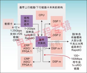
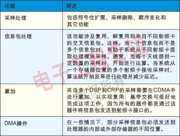
Table 1: Functions performed by the system in the baseband switch.