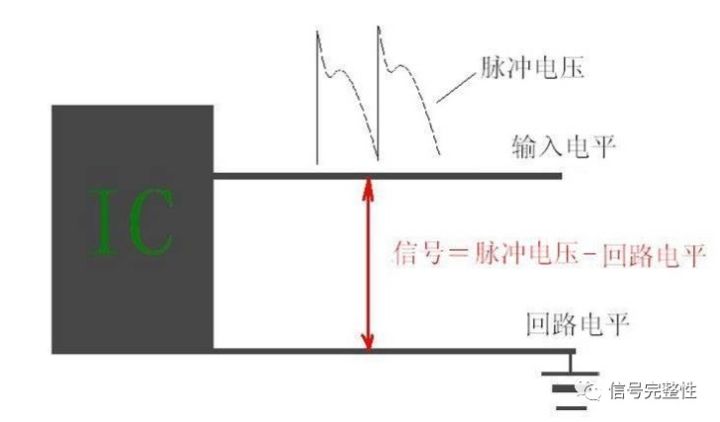
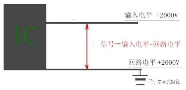
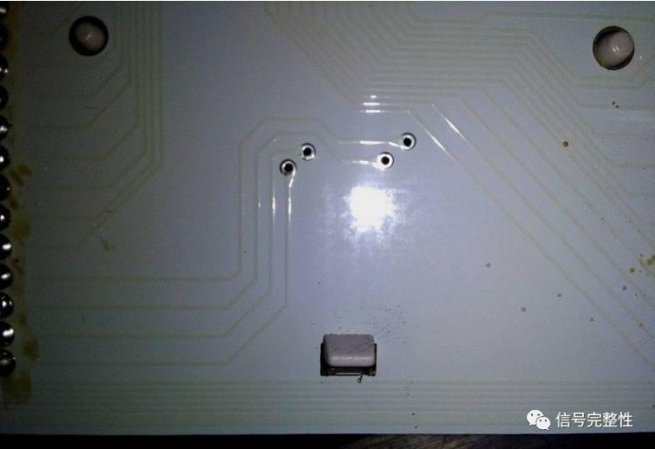
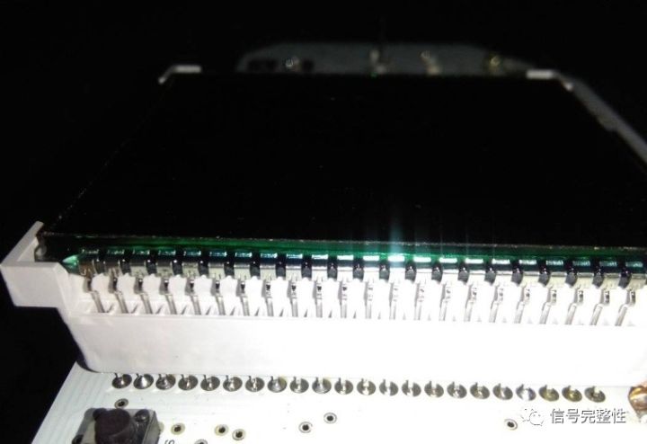
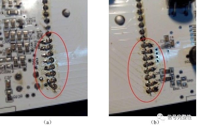
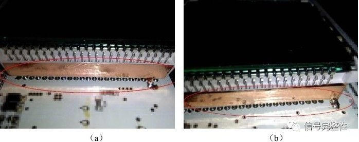
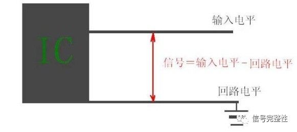
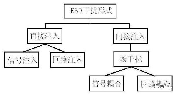
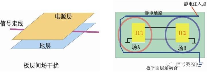
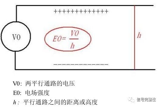
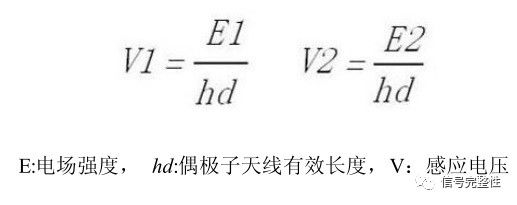
1. Description of the phenomenon When the product carrying air 25KV ESD immunity test, the discharge slit to the display screen immediately below the location of the meter housing, the instrument panel LCD display character error, breaking yards, and so the video, shown in detail in Figure 1 below: Figure 1 Air discharge experiment 2. Reason analysis First, we analyze the principle of signal formation. When a level is input, it is necessary to distinguish whether it is a useful signal or an unwanted signal. In short, to determine the level, polarity, frequency, and other parameters of a signal, an overall reference level must be used as a reference. In the circuit design, we use the current loop as the reference level reference for a single system, which is the 0V level. As shown in Diagram 2, the signal is equal to the input level minus the reference level, and the resulting signal level may be positive or negative. As long as the reference level of a single unit loop is consistent and stable, the entire circuit unit can operate normally according to the original design specifications.              figure 2 In EMC practice, there are many types of electrostatic interference, coupling methods, coupled pulse voltages, and polarities. Basically, there are two types of direct interference and indirect interference from the discharge route. The two basic forms of signal interference and loop interference are shown in Figure 3 below. image 3   The test phenomenon of the automotive instrument assembly is to discharge air 25KV level to the gaps around the display screen, display errors or abnormal work. Corresponding to Figure 5, we can find the basic form of air discharge interference - that is, electrostatic field interference. At this point it is also necessary to analyze how this electrostatic field causes the system to work abnormally, how to couple it to the internal circuit system, and whether the signal path or the loop is disturbed. Only by thoroughly understanding the cause can we fundamentally treat the disease. Corresponding to the above-mentioned test phenomenon, several types of electrostatic interference can be analyzed with the help of schematic diagrams 4 and 5 . Figure 4 Figure 5 FIG 4 shows a schematic view of an electrostatic field formed between a plurality of plies schematic interference, a multilayer PCB board, often a lot of signal lines are laid down in the adjacent layer or an intermediate layer or formation of a power supply layer, according to our A lot of experimental analysis proves that in the electrostatic discharge immunity test, once the impedance of the release route of the formation is large, the signal layer or power supply of the adjacent layer is easily coupled to the static electricity site formed on the formation. Similarly, the principle of the electrostatic field formed by the power layer is similar. In Fig. 4, the failure factor caused by the multilayer PCB is mainly considered. As shown in Figure 5, the single-sided or double-sided structure distribution is more common. Due to the PCB traces or the surrounding floor structure, the electrostatic pulse voltage is directly or indirectly injected into the static electricity generated by the loop. In the field distribution, the system or unit module in the electrostatic current loop will be coupled to the field energy. If there are multiple units or modules, the electrostatic field energy coupled to each unit or module will be based on the layout of the PCB structure. It's different. In Figure 4 and Figure 5, in theory, the equivalent of Figure 6 can be used to help analysis. Figure 6 The electric field E0 is equal to the distance h from V0 to the upper two parallel paths. In actual production and work, we will find that due to the influence of the structure of the traces, the cross-sectional area of ​​the conductors, the distribution of devices, and the resistance of the vias, multiple field distributions with different intensities will result, as shown in Figure 5. Two field distributions with different intensities of electrostatic field A and electrostatic field B are formed. The two cell modules IC1 and IC2 in the field distribution will be interfered by two electrostatic fields of different intensities, assuming the middle of IC1 and IC2 in the field distribution. The line looks like a dipole antenna, and the effective length is hd. According to the theoretical formula, two different voltage values ​​can be sensed on its trace. Let the electrostatic field A be E1 and the electrostatic field B be E2 because of E1. ≠E2, set the effective antenna lengths of the two units to be the same (in reality, the two unit modules can never be the same), and finally get V1 ≠V2. The calculation method is as follows:                 When the induced V1, V2 energy is high enough and △V1V2 is large enough, the normal communication signal between IC1 and IC2 can be disturbed. According to the analysis of previous Figure 2, the signal at this time is equal to the signal sensed on the signal line. The pulse voltage minus the loop level is shown in Figure 7. At this point the circuit has failed to identify the signal, causing the circuit to work abnormally.                            Figure 7 3. Corrective measures Through the above theoretical analysis, the fault factors of the product are mainly caused by the electrostatic field interference. To solve the field interference problem, there are two general methods: First, use the bleeder method to effectively perform the “antenna†on the sensitive Decoupling processing, in the signal path for the release, to achieve the purpose of passing; second is the use of shielding methods, the sensitive unit module, "antenna" and other necessary electrostatic shielding, to ensure that the difference between the signal and the reference level is not Mutations occur to make it work. No matter what kind of technical scheme we use, its fundamental purpose is to eliminate the difference between the signal level and the loop reference level. As shown in FIG. 8 below, the input level and the loop level of the unit circuit are kept increasing or decreasing at the same time, and the total difference of the signal level can be maintained substantially unchanged. Figure 8 Static devices such as TVS, discharge tubes, varistors, high-molecular absorption materials, and capacitors are commonly used. For the signal port, the most effective, the lowest cost, the most reliable performance is still the choice of capacitors, the use of capacitors on the transient characteristics of the pulse signal can quickly discharge the static pulse to the direction of the low potential, to achieve the purpose of balance . The internal structure of the product is further analyzed. Figure 11 shows the signal traces of the LCD panel. The traces are long and there is no ground in the blank position. There are more blank areas. In the case of electrostatic discharge, the antenna can be easily formed by the traces.                  Figure 9 shows the alignment of the data lines      Figure 10 shows the connection structure between the LCD and the motherboard. The plug-in type has a high distance of about 1cm. The LCD data pins may also form antenna effects and receive electrostatic field disturbances. Figure 10 Pin Structure Diagram of LCD Screen Through the analysis of the basic circuit structure, when the PCB layout, especially in the design of the data trace of the LCD screen, there are deficiencies, the trace is long, and the trace gap and the chip periphery are not paved, there is no isolation and absorption As for the stratum, the LCD is similar in terms of assembly structure. The plug pins are too long and no decoupling measures are added. As a result, all the data lines in the discharging process become the receiving antennas. A slight improvement in the design can pass the test, but the customer's product has been produced, and the PCB will not undergo major changes later. Therefore, the rectification plan formulated is to adjust or add devices without changing the PCB board, and to ensure the cost and process feasibility. According to the foregoing principles, formulate a rectification plan: 1. For the important data lines close to the edge, decoupling techniques are used to reduce the receiving capacity of the “antenna†so that it can form a discharge path to the ground and achieve the purpose of suppressing static interference. Use a 100pF capacitor on the LCD pin in parallel with ground, as shown in Figure 11; Figure 11 Data Line Decoupling 2. Shield the traces. Since the pin is too long, the electrostatic field of the screen mask processing pin, eliminating electrical fields in the left and right LCD holder pin, and a good grounding shielding copper foil is employed, for absorbing static electrical interference. The shielding measures can be changed in the redesign of the PCB traces and the grounding around the LCD pins instead. Figure 12 LCD Screening 4. Test verification 25KV electrostatic discharge test passed. 200*300mm Anti-Blue Light Film
The Imported Anti-Blue Light For ipad is made of high-quality imported TPU material. It is precisely cut by the Screen Protector Cutting Machine. Protect your device screen from scratches and cracks. The flexible TPU Screen Protector can completely cover the iPad screen, providing the maximum protection for the iPad.
Advanced blue light blocking technology can protect your eyes, can effectively filter blue light, prevent glare, reduce eye fatigue, and help you fall asleep better.
Super clear and transparent, will not reduce the screen brightness, maintain the original screen brightness, and reduce eye fatigue.
The Protective Film adopts an oleophobic and waterproof coating, which can ensure anti-fingerprint, waterproof, dustproof and no air bubbles. Moreover, it is sensitive to touch, bringing natural touch, fast response and flawless precise touch.
If you want to know more about Imported Anti-Blue Light For ipad products, please click product details to view the parameters, models, pictures, prices and other information about Imported Anti-Blue Light For ipad products.
Whether you are a group or an individual, we will try our best to provide you with accurate and comprehensive information about Imported Anti-Blue Light For ipad!
Imported Anti-Blue Light Protective Film, Imported Anti-Blue Screen Protective Film, Imported Anti-Blue Screen Protector, Imported Anti-Blue Light Screen Protector Shenzhen Jianjiantong Technology Co., Ltd. , https://www.jjtscreenprotector.com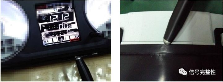
 Â Â
 Â Â Â