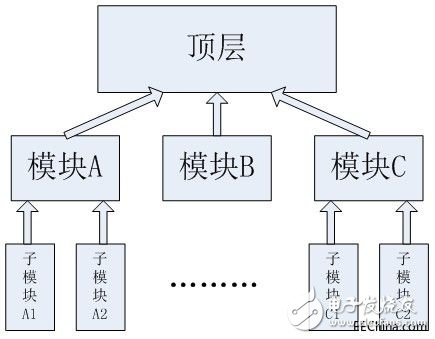
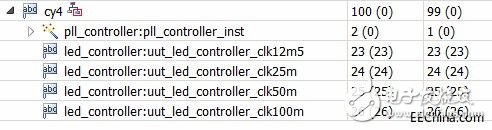
Modular design is a very important skill in FPGA design. It can make division and collaboration of a large design, simulation testing easier, and code maintenance or upgrade more convenient. As shown in Figure 8.28, the top layer of the entire design is typically instantiated and not logical. Then there will be a module A, a module B, a module C, and so on under a top layer. The module A/B/C can be divided into a plurality of sub-modules. Figure 8.28 Module Level Design In this way, large-scale and complex systems can be divided into several modules according to certain rules. Then each module is designed for input and synthesis, and the implementation results are constrained in a pre-set area, and finally the results of all modules are realized. Organized organically, you can complete the design of the entire system. For the design of the top-level module, the competent designer needs to complete the design input and synthesis of the top-level module and prepare for the first step of the modular design implementation phase, the initial budget phase (IniTIal BudgeTIng Phase). For the design of the sub-modules, the designers of multiple modules complete the design input and synthesis of the respective sub-modules in parallel independently, and perform the sub-module activation mode implementation (AcTIve Module ImplementaTIon) for the second step of the modular design implementation stage. ready. The modular design implementation step is the most important and special in the entire modular design process. It includes: â— The initial budget, this stage is the first step in the implementation of the steps, and plays an instructive role in the entire modular design. In the initial budget stage, the project manager needs to position the overall layout of the design. Only when the layout is reasonable, can the advantages of the modular design be reflected to the greatest degree; otherwise, if the layout is unreasonable, it needs to be performed again at a later stage. The initial budget requires a complete rework of the entire implementation step. â— Active Module Implementation of sub-modules. At this stage, each project member completes the implementation of their respective sub-modules in parallel. Final assembly of the module. At this stage, the project manager organically organizes the implementation results of the top layer and the activation patterns of all the sub-modules, and completes the implementation steps of the entire design. The basic principle of module division is that the sub-module functions are relatively independent, the internal links of the module are as close as possible, and the connection between the modules is as simple as possible. For complex designs with strong internal correlations that are difficult to meet the module partitioning criteria, modular design methods are not suitable. In this experiment, we are going to experience a modular design. As shown in the figure, in this design, our top-level module is cy4.v. In the previous example, we have only a single cy4.v is the source code file, and all the logic code is written in this file. , But this example begins, we will use the modular design, write each different independent functional logic code in different source files, and then through the "instantiation" way, interconnect the interfaces between them. Therefore, in this example, the cy4.v file actually has almost no specific logic function. It just does some basic instantiation and interconnection and connects the interface signals related to the five function modules below it. As shown in Figure 8.29, they also have a specific hierarchical relationship, which is very easy to see and edit. Figure 8.29 Module hierarchy diagram 2 board debugging Referring to the previous example, the sp6.bit file generated by this example is burned into the FPGA. Then we can see that the four LEDs D2, D3, D4, and D5 flash in full synchronization. Of course, this also at least proves the quadrature relationship between the four clocks of our PLL output.
HIGH QUALITY:Made of only the highest quality materials and built to last! Our chargers are gauranteed to match the original brand name chargers' quality.
EASY TO USE: Simply plug the charger into a wall outlet and then directly into your scooter.
The charger protected: Short circuit protection/ over current protection/ over voltage protection; red light -- charging, green light -- charge OK, it stop automatically when the battery is full. Warm Tips: To avoid the temperature of your charger too high, please do not charge too long.
Aviation Plug Scooter Charger,Power Scooter Charger,Li-Ion Battery Charger Shenzhen Waweis Technology Co., Ltd. , https://www.laptopsasdapter.com