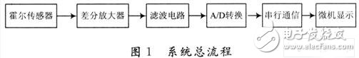
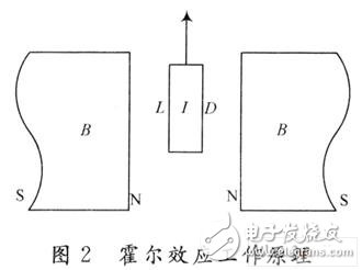
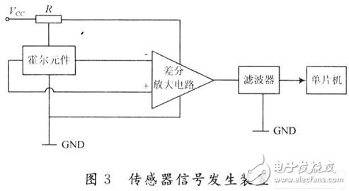
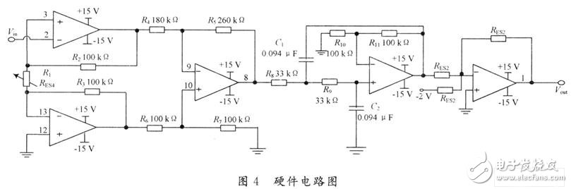
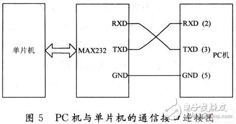
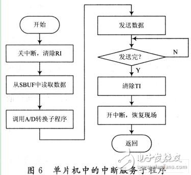
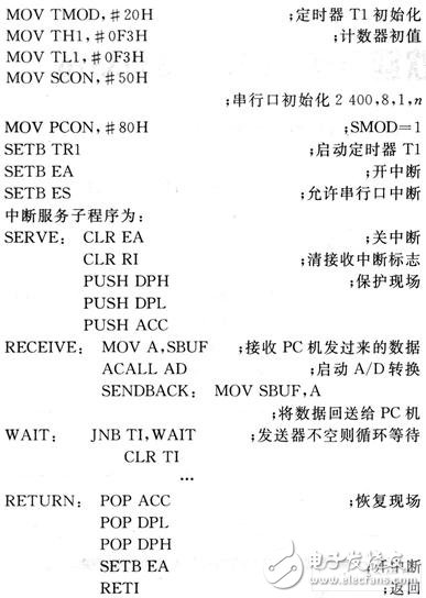
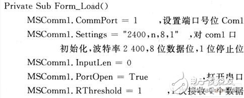
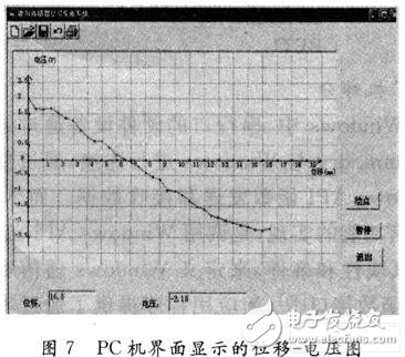
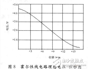
In recent years, with the development of sensor technology and the wide application of single-chip technology, more and more small-scale sensor measurement and control systems composed of single-chip microcomputer and PC are used. Introduction In recent years, with the development of sensor technology and the wide application of single-chip technology, more and more small-scale sensor measurement and control systems composed of single-chip microcomputer and PC are used. The key is that they combine the advantages of low price, strong function, good anti-interference ability, wide temperature limit and control-oriented, as well as advanced user interface, multi-tasking and automatic memory management of Windows in Pc machine operating system. In this kind of measurement and control system, the MCU mainly performs real-time data acquisition and pre-processing, and then sends the data to the PC through the serial port. The PC then further processes the data, such as averaging, variance, drawing dynamic curve and calculation. Tasks such as setting and printing various parameters. Here, the Hall sensor is used as the front end for data acquisition, and then A/D conversion is performed under the control of the single chip microcomputer, and the signal is sent to the PC through the serial port for drawing processing. 1 System introduction The system can be divided into 3 parts. The first part is the signal source. The voltage signal is generated by the Hall sensor. The signal is amplified by differential amplification to obtain a clearer signal. The second part is that the signal is sent to the MCU for processing after A/D conversion, and then sent to the PC through serial communication. The machine process gets the result; the third part is the display of the data, which is done by the VB drawing program, and the display result is displayed in the vx diagram. The overall system flow is shown in Figure 1. 2 hardware design and implementation 2.1 Hall sensor The Hall sensor is a sensor that realizes magnetoelectric conversion using the Hall effect. It has high sensitivity and wide application characteristics. The working principle is shown in Figure 2: a semiconductor wafer with a length L, a width B, and a thickness D, placed in a magnetic field with magnetic induction B, with a control current I on both sides, and the magnetic field direction If the current direction is orthogonal, a potential U proportional to the product of the control current and the magnetic induction intensity will be generated on both sides of the semiconductor. The potential is the Hall voltage, expressed as UH, ie UH=KHIB, where KH is the Hall element Sensitivity, the semiconductor wafer is the Hall element. Similarly, there are two permanent magnets with the same magnetic field, which are placed opposite to each other. When the surface area is much larger than the spacing between the two, the positive intermediate magnetic induction is O, and a uniform gradient magnetic field dB/dx=K (K is constant) is formed along the z-axis between the slits. B=0 is the reference origin of the displacement x, then when x=O, B=O, UH=O. When the Hall element in between them moves to x, the UH size is determined by B at x. It can be known from the formula UH=KHIB that dIH/dx=IKHdB/dx=KHI=K, and UH=Kx after integration, that is, the Hall potential is proportional to the displacement. The larger the magnetic field gradient, the higher the sensitivity, the more uniform the magnetic field changes, and the better the linearity of UH and x. The first part of the system is provided by the Hall sensor device of Figure 3 and consists of a Hall element (A44E), a differential amplifier and a filter. Its output voltage is proportional to the displacement of the Hall element and has a high sensitivity to generate a voltage signal that meets the requirements. 2.2 Analog-to-digital conversion principle The microcontroller in this system uses Atmel's AT89C51 microcontroller and is compatible with MCS-51 microcontroller products. It has 4 KB flash programmable erasable read-only memory, 1 000 erase and write cycles, and 32 programmable I/Os. Port line, two 16-bit timer/counter, five interrupt sources, UART serial channel, etc. It is mainly used in the design to control the analog signal output from the sensor signal generating device to be converted into a digital signal for data acquisition and display as well as serial communication. A converter that converts the analog quantity processed by the standard amount into a discrete signal expressed by a binary value, referred to as an A/D converter. The input of the converter is generally DC current or voltage, and the output is a digital quantity of binary digits. The ADC0809 converter is used in this design. The process is as follows: First, it can be seen as a combination of an 8-bit A/D converter and an 8-channel analog multiplexer. INO~IN7 correspond to 8 analog inputs, respectively, by pins ADDA, ADDB and ADDC decides which analog quantity to convert. After adding a positive pulse to the START and ALE pins, the channel select code is immediately locked and the ADC conversion is initiated. After the start of the conversion, a positive pulse is added to the OE pin to turn on the tri-state gate of the output buffer, so that the converted digital quantity can be transferred to the data bus. 2.3 Data collection and display After the amplified voltage signal reaches the range that can be processed in the amplitude, the range of the analog-to-digital voltage conversion is 0 to 5 V, and the voltage output from the sensor has a negative value. In order to match the voltage, the signal voltage is A first-stage addition circuit can be added before the analog/digital converter is connected, and the voltage signals are all converted into positive values. The amplifying circuit, the filtering circuit and the adding circuit are all implemented by LM324, and the hardware circuit is shown in FIG. 4. The data display circuit is divided into a digital tube display circuit and a PC display portion. The digital tube display is used on the single chip microcomputer, and the single chip computer controls the data displayed on the digital tube through the segment display code and the bit display code respectively. The segment display code controls the displayed data content, and the bit display code controls the digital tube to be on or off. The segment display code is transmitted to the 8-bit shift register 74LSl64 bit by bit through the programmable universal parallel interface 8155, and then it converts the serial transmission data into parallel data and transmits it to the digital tube display. The bit display code is that the MCU latches into the data latch 74L$244 through the 8155 at a time, and then drives the digital tube and controls its light or off. 2.4 Serial communication The design uses asynchronous serial communication. The serial port of the AT89C51 MCU, when working in modes 1, 2 and 3, UART (Universal Asynchronous Receive and Transmit) can realize serial communication between the MCU system and the PC. The serial communication of the PC is mainly realized by the serial port chip 8251. The 8251 has 10 registers with port addresses from 3F8H to 3FEH (c0M1). The 8251 can be programmed to specify the communication protocol, ie the baud rate, number of data bits, parity type and stop bit length of the communication. In addition, since the level of the serial port of the PC is RS 232 level, it is not compatible with the TTL level of the serial port of the MCU, so it is necessary to perform level conversion between them. The traditional method is to use MCl488 to convert TTL level to RS 232 level and reverse conversion with MCl488. Since the MCl488 requires ±12 V voltage, it is very inconvenient to use, so the design is implemented by MAXIM's product chip MAX232. Powered by a single +5 V voltage, it can realize TTL to RS 232 level conversion, and also realize RS 232 to TTL level conversion. It is very convenient to use. The specific circuit is shown in Figure 5. 3 software implementation part 3.1 MCU part The serial port of the AT89C51 series MCU can work in 4 different ways. In this program, the serial port operation of the MCU is set to mode 1, that is, the data is transmitted through the TxD terminal, the RxD terminal is received, the baud rate is 2 400 b/s, 10 bits constitute one frame, l bit start bit, 8 bits. Data bit, 1 stop bit, initial value 0F3H, SMOD=1. Since the single-chip microcomputer is mostly used in a control situation with strong real-time performance, in order to minimize the CPU time, the CPU function is fully utilized. The system uses the interrupt mode to communicate with the PC in the microcontroller program design. The main program only performs serial communication, digital tube real-time display, initialization of analog/digital conversion results, and cyclic wait for serial interrupt operation. When receiving a signal from the PC, it transfers to the interrupt service routine for A/D. Convert and send data to the PC. The interrupt service subroutine flow chart is shown in Figure 6. The serial communication initialization and interrupt service subroutine code is only given below: The serial communication initialization procedure is: 3.2 PC part In Windows, the serial port hardware device connects to Windows via the communication driver comm.drv, and sends and receives data using standard Windows API functions. The communication function of the MSComm control is to call the windows API function, and define the API function interface of the windows communication driver by setting its properties and events, providing an easy way for the application to send and receive data through the serial interface. The MSCOmm control provides two ways to handle communication: one is the event-driven method, which is to use the OnComm event, which is a very efficient way to handle serial port activity, not only to detect and handle communication events using the MSCOmm control. Error, but also has the advantage of timely response, high reliability; another method is the query method, the C0mmEvent property of the MSComm control returns the event and error type generated in the communication, and is set by the communication control to automatically detect and track the communication status. Therefore, you can directly read the value of the CommEvent property to detect the types of events and errors generated in the communication. This method is relatively simple and is commonly used in small self-contained programs. The design program uses the query method to read the attribute value of InBufferCount to receive the data sent by the microcontroller. The main program of the experiment initializes the serial port and draws the coordinate system; each clicks the 'paint point' key program to send an arbitrary number to the single-chip microcomputer, tells the single-chip microcomputer to send the analog-digital conversion result, and then receives the data by query method, and performs corresponding conversion. Then draw the point on the coordinate system and the data acquisition ends. Common properties of the MSComm control: CommPort: Set and return the communication port number; SetTIngs: Set and return the baud rate, parity, data bits, stop bits in the form of a string; Pott() pen: Set and return the communication port The state can also open and close the port; Input: return and delete characters from the receive buffer; Output: write a string to the transfer buffer. The experimental Coml port serial communication initialization procedure is as follows: From the PC interface in Figure 7, the displacement-voltage graph is displayed, the data recorded in Table 1 and the ideal voltage-displacement graph of the Hall linear circuit shown in Figure 8 on the oscilloscope are compared. It can be found that the sensor bench is affected by external interference. The reason is that the output signal output error is inevitable, and there is no level shifting, so that the value obtained in the VB plot has a negative value; but it can be seen in the figure that the voltage value of the sensor output has obvious symmetry between positive and negative, It is consistent with the ideal output signal waveform of the required output, which proves that the system works well and the design is very successful. 4 Conclusion It has important reference value for realizing the communication problem between PC and MCU in the widely used WindOWs environment. Others Washing Machine Motor,Drain Motor Washing Machine,Washing Machine Dryer Motor,Inverter Motor Washing Machine WUJIANG JINLONG ELECTRIC APPLIANCE CO., LTD , https://www.jinlongmotor.com