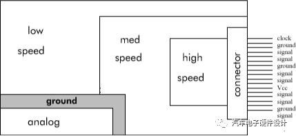
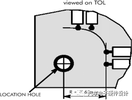
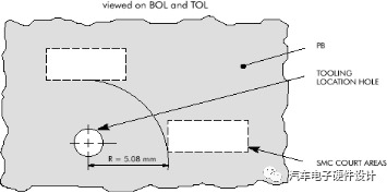
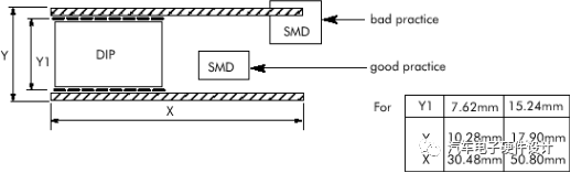
For a designer to consider the distribution of PCB components to consider the following diagram. A. High-speed components (and external interfaces) should be as close as possible to the connector. B. Digital circuits and analog circuits should be separated as much as possible, preferably separated by ground. 3. Spacing between components and positioning holes A. The distance from the positioning hole to the nearby pin pad is not less than 7.62 mm (300 mils). B. The distance from the positioning hole to the edge of the surface mount device is not less than 5.08mm (200mil). For SMD components, the minimum radial distance from the center of the positioning hole center SMD component is 5.08mm (200mil) 4) DIP automatic plug-in machine requirements. On PBs with both SMD and DIP components, to avoid damage to DIP components during automatic insertion SMD components must consider layout requirements for SMD and DIP components when laying out. Stage Display,Rgb Laser Animated Light Show,Lighting Wall Lamp For Outdoor Building,Residential Holiday Lights Kindwin Technology (H.K.) Limited , https://www.szktlled.com