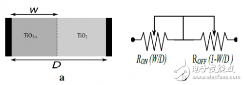
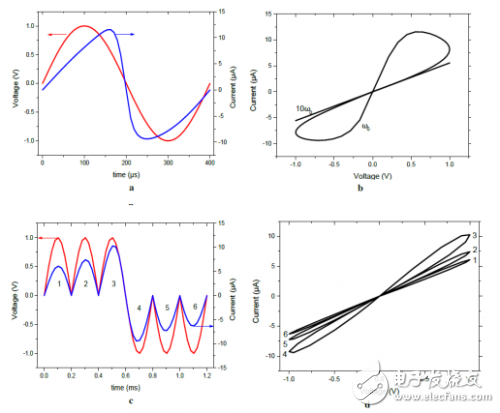
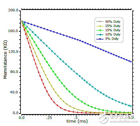
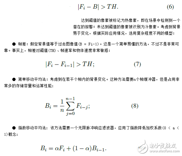
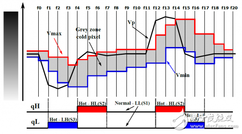
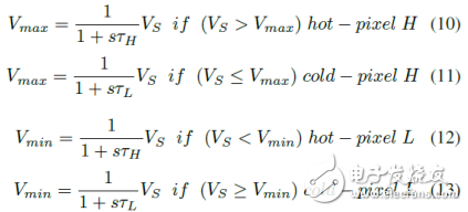
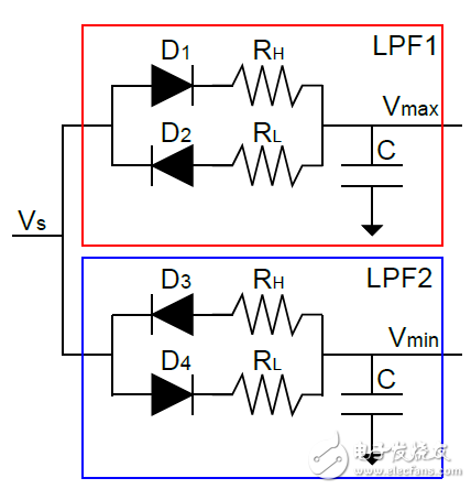
This paper introduces an imaging sensor architecture that relies on a memristor to perform a pixel-level adaptive background extraction algorithm. The pixels of the built-in optical frequency converter (L2F) are the core components of image processing. When the digital pulse whose output is proportional to the light intensity is applied to the memristor, the memristor resistance will change accordingly. The other two memristors are used to preserve the dynamic boundary, and the behavior of the photo-generated signal outside the boundary is considered to be an abnormality, that is, an unexpected rapid change. Compared to full CMOS imaging sensors, memristor-based solutions enable smaller pixel pitch and non-volatile storage, allowing designers to create image background models using programmable time constants. 1 Introduction In the past few decades, the industry has carried out extensive research and discussion on the CMOS visual sensor theory, aiming at processing images in the early stages of imaging, extracting the most important features from the scene, and if other methods are used for the same purpose, for example Using common computing techniques requires expensive costs. In this respect, motion detection is one of the most important image features and the basis for multiple complex visual tasks. This article focuses on the concept of time contrast, a concept that is especially important in many applications, including traffic monitoring, human motion photography, and video surveillance. These applications require accurate and reliable image detection, accurate shape detection, and timely response changes. In addition, motion detection must be flexible to adapt to different work scenarios and light intensity conditions. Background extraction is currently the most recognized method of motion detection. Background extraction is to generate a background estimate and then update it frame by frame. Analyze the type of motion and associate it with a specific object in the scene for a higher level of processing. In the process, the change in light intensity is undoubtedly the first clue to help us discover the movement. Because it is possible to accidentally detect all pixel changes at a certain point in time, including changes caused by light, shadows, and noise, potential changes that should be considered when the pixel changes too fast relative to the past. Therefore, a low-pass memory should be implemented at the pixel level to track pixel contrast changes and alert when pixel behavior changes. This article describes how to implement the above algorithm using a memristor. In the 1970s, Professor Cai Shaozhen theoretically predicted the existence of a passive device called a memristor. In 2008, HP Lab demonstrated the physical model of this passive device. In the name of the memristor, the memristor is a kind. A variable resistor whose on-state can memorize the current history of the previous flow through the memristor. The main contents of this paper are as follows: The next chapter introduces the memristor behavior related to input bias, especially pulse-based programming, which is the basis of this paper. The third chapter introduces the working principle of pixels, and the fourth chapter focuses on pixel implementation. The fifth chapter introduces the simulation results, and the sixth chapter is the conclusion. II. Memristor behavior As mentioned earlier, the memristor can be viewed as a time-variable resistor, the value of which depends on the current value previously flowing through the memristor. Figure 1: Memristor and simplified equivalent circuit diagram. Figure a: TIO2 memristor structure; Figure b: equivalent resistor circuit The first proposed memristor concept is Professor Cai Shaozhen, who believes that the memristor is the fourth basic passive component other than resistors, capacitors, and inductors when inferring the symmetry basis of the passive circuit theory. After discovering the physical model of the memristor, many people want to develop analog integrated circuits using the exciting memory characteristics of the memristor. The first physical model developed by HP Labs is based on two regions of TIO2: a high-resistance undoped region and a doped region with highly conductive oxygen holes TIO2-x sandwiched between two metal electrodes In the middle of the board, as shown in Figure 1a. When an external bias is applied to the memristor, the boundary between the doped layer and the undoped layer moves, and the displacement is a function of the applied current or voltage, and thus the drift of the charged doped region results in two The resistance between the electrodes changes. For simple resistance conduction, the following equation defines the voltage-current relationship: Using the reference to obtain the parameters related to the above equation, a memristor behavior model was developed using Verilog-A language. Through the circuit simulation, the model was verified by the following parameters: RON = 200Ω, ROFF = 200KΩ, u2 = 10-10cm2S- 1V-1, D = 10nm. As long as the system is within the M? (RON, ROFF) boundary, the memristor exhibits symmetrical behavior. When any boundary is reached, the memristor will act like a linear resistor, keeping the boundary resistance until the input polarity is reversed. Figure 2 shows a typical memristive characteristic curve. These interesting behaviors of the memristor together constitute the basic characteristics of a memristor or a variety of memristive devices. Figure 2a is a plot of applied voltage and corresponding current versus time t. Figure 2b shows the current-voltage characteristic curve. It is not difficult to see from the figure that when w ≤ w0, hysteresis occurs, and when w? w0, the lag is shortened. Figure 2c shows the behavior of the memristor under unbalanced input signal conditions. We observed that during the first three cycles, the w(t) value gradually increased, which is the result of the accumulation of net charge over a certain period of time. After three consecutive cycles of opposite polarity signals are applied, w(t) is reduced to the initial state. In summary, as shown in Figures 2a and 2b, any symmetrical AC bias can cause double-loop current-voltage hysteresis, dropping to a straight line at high frequencies. Furthermore, for any asymmetry in the presence of a bias voltage, as shown in Figures 2c and 2d, we observe a multi-ring current voltage hysteresis, and as the current increases, the multi-ring current voltage hysteresis becomes more pronounced. Figure 2: Behavioral simulation results of a voltage-driven memristor. In Figure a, the applied symmetrical input voltage (red) and the corresponding current (blue) are a function of time. Figure b is a symmetrical input current-voltage characteristic curve. The descending line corresponds to a curve with a higher curvature. In Figure c, the asymmetric input applied voltage (red) and the corresponding current (green) are a function of time. Figure d is an asymmetrical input current-voltage characteristic curve. The applied voltage in Figure a is ±v0 sin(w0t), and the applied voltage in Figure c is ±v0 sin2(w0t), where w0 = 2?f0 = 2?u2/D2. The memristor's initial resistance is usually large, and applying a continuous or pulsed voltage of opposite polarity linearly reduces the resistance to a low-resistance valley, as shown in Figure 3. Applying a voltage of opposite polarity restores the memristor to its initial high resistance, which is usually much shorter than the direct recovery method. In FIG. 3, the initial resistance value of the memristor is very high, and a series of duty cycle controllable pulse frequency wp=5w0 and current amplitude ip=160uA current pulse are applied to the memristor, so that the memristor can be applied to the memristor. data input. The higher the duty cycle, the greater the amount of charge flowing through the memristor and the faster the conduction speed. The memristor has a pulsed nonlinear programming function. The optical frequency converter is used as a programming signal source, and the memristor is driven by a current pulse proportional to the light intensity to realize photoresist (L2R) encoding. As shown in the pixel structure diagram of FIG. In addition to its unique non-linear programming, the memristor can be viewed as both a storage effect of the capacitor and a leakage-free electrical resistance of the resistor. All of this, combined with its small size and ease of implementation, makes it one of the most interesting analog signal processing application components, but this article only discusses how to use the memristor to perform background extraction in a compact pixel. Figure 3: Membrane-time change rate when programming a resistor with a series of different duty cycle programming frequencies wp=5w0, current amplitude ip = 160uA III. Working principle Before discussing the sensor architecture, we need to describe the pixel-level adaptive background extraction algorithm. We consider the case where one pixel of an imaging sensor encodes a particular scene point. The pixel acquires the light intensity at a frame rate fps and converts it into a voltage VS(nT), where T = 1/fps is the pixel sensor sampling time and the integer n represents the number of frames. During the operation of the sensor, the intensity of the light collected by the pixel changes dynamically, and the rate of change depends on the type of motion within the scene or the change of ambient light. By monitoring the dynamics and amplitude of the signal, each pixel needs to check for potential anomalies in the scene. To do this, the background (B) must be extracted from the existing image (Fi) and then the final difference and the correct threshold (TH) are compared: The main advantage of this method is that the memory can be fine-tuned by changing the learning rate value a without adding memory. Considering the hardware implementation problems and robustness of the above method, we use the exponential moving average method and two voltage thresholds instead of a threshold pressure of reference (6) to establish a background model. The threshold voltage defines the voltage range over which the signal can change safely (cold pixels) beyond which the signal is considered to be abnormal (hot pixels) and may trigger an alarm. Figure 4: Performing a background dynamic extraction algorithm at the pixel level Figure 4 shows the working principle of the background extraction algorithm. This example is how a single pixel works during 20 frames. The black curve represents the signal voltage VS acquired by the pixel, and the red line (Vmax) and blue line (Vmin) waveforms are sets of two threshold pressure values ​​defining the upper and lower boundaries of the gray area. In the gray area, the signal can be freely changed without any occurrence. Call the police. The signal voltage VS is low-pass filtered to generate a signal, and each filter switches between two time constants (tH < tL) depending on the following conditions: Where equations (10) and (12) represent the hot pixel conditions of Vmax and Vmin, respectively, while equations (11) and (13) represent the cold pixel condition. The behavior of the two thresholds defines a gray region that varies according to the dynamics of the signal over a period of time. The gray region represents the voltage range of the motion in which the VS has not found an abnormal condition. For example, if the VS suddenly dims from bright to dark, it crosses the upper boundary of the gray region ( Vmax), a hot pixel is generated. Figure 5: Two first-order low-pass filters generate the two threshold voltages in Figure 4. Adapter Fiber Optic Box,Multimode Fiber Adapter Coupler,All-In-One Fiber Optic Adapter Coupler,Full Complement Fiber Optic Adapter Coupler Shenzhen Jingtu Cabinet Network Equipment Co., LTD , https://www.jingtucabinet.com