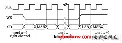
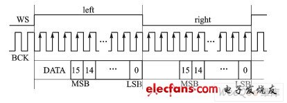
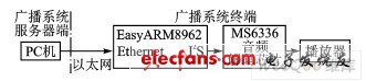
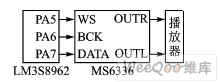
introduction I2S (InterIC Sound Bus) is a bus standard developed by Philips for audio data transmission between digital audio devices. It uses a separate wire to transmit clock and data signals. By separating data and clock signals, the time difference is avoided. Induced distortion. The I2S bus is simple and effective, can effectively improve the quality of output data, and is widely used in various embedded audio systems. However, in the embedded audio system design, not all MCUs support the I2S bus format. In addition, I2S does not have a unified interface standard. The device interfaces produced by different manufacturers are also varied. The software simulation can realize the I2S bus. A problem that occurs when data is transmitted over an I2S bus between an MCU and a device that does not support it. In this paper, the voice data transmission is realized by software simulation I2S bus in Ethernet digital voice broadcasting system, and the method of software simulation to realize I2S bus is given. 1 I2S bus specification I2S is a three-wire bus, and the three signals are: 1 Serial clock SCK, also called bit clock (BCK). That is, every time you send 1 digit of digital audio data, there is 1 pulse on SCK. SCK frequency = 2 & TImes; sampling frequency & TImes; number of samples. In the data transmission process, the transmitter and receiver of the I2S bus can be used as the host of the system to provide the clock frequency of the system. 2 Frame clock WS, command (channel) selection, used to switch the data of the left and right channels. The frequency of WS is equal to the sampling frequency and is provided by the system host. A WS of "0" indicates that the data of the left channel is transmitted, and a WS of "1" indicates that the data of the right channel is transmitted. 3 Serial data signal SD for transmitting audio data represented by two's complement. Signals of the I2S format No matter how many bits of valid data, the most significant bit (MSB) of the data bit is always transmitted first, and the data that can be transmitted once is determined by the effective number of bits in the I2S format. A typical I2S signal timing is shown in Figure 1. Figure 1 I2S bus typical timing diagram With the development of technology, a variety of different data formats have emerged under the unified I2S interface. According to the difference of the SD signal with respect to the position of SCK and WS, it is divided into two formats: left-aligned and right-aligned, as shown in FIG. 2 and FIG. Figure 2 Left-justified format of 16-bit significant digits Figure 3 Right-aligned format of 16-bit significant digits In the above two data transmission formats, when the WS is "1", the data of the left channel is transmitted, and when the WS is "0", the data of the right channel is transmitted. In order to ensure the correct transmission of digital audio signals, the sender and receiver must use the same data format. 2 software simulation I2S The Ethernet digital voice broadcasting system mainly refers to a broadcasting system that provides audio services by using Ethernet as a propagation medium, and transmits voice signals on the Ethernet in the form of standard IP packets to implement a voice broadcasting function. The system collects voice data through the microphone on the PC end, and then sends the collected voice data to the embedded terminal through the Ethernet, and the embedded terminal performs digital/analog conversion on the received voice data to play. The system implementation block diagram is shown in Figure 4 [5]. Figure 4 Block diagram of the Ethernet digital voice broadcasting system Figure 5 Connection diagram of LM3S8962 and MS6336 The MCU LM3S8962 of the broadcast system terminal sends the received voice data to the voice decoding chip MS6336 through the I2S bus for digital-to-analog conversion and playback. The connection between the LM3S8962 and the MS6336 is shown in Figure 5. In order to completely restore the voice signal, it is necessary to ensure that the software analog I2S signal timing is strictly accurate, and the high and low level conversion is implemented by a delay program. The MS6336 is a 16-bit D/A chip, and its I2S timing is shown in Figure 6. Figure 6 Typical I2S timing diagram for the MS6336 The voice data in the system is two-channel, 16-bit sampling, and the data of one sampling point is 4 bytes, and one sampling point data is sent to the MS6336 through the MCU, and the data transmission process is as shown in FIG. 7. Figure 7 1 sample point data transmission process Fork Type Connecting Terminals Fork Type Connecting Terminals,Terminals,Connecting Terminals Taixing Longyi Terminals Co.,Ltd. , https://www.longyicopperlugs.com