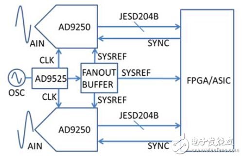
Many communications, instrumentation, and signal acquisition systems require simultaneous sampling of multiple analog input signals through multiple analog-to-digital converters (ADCs). The sampled data is then processed to synchronize the individual channels, however they each have different delays. This has long been a problem for system engineers using LVDS and parallel output ADCs. JESD204B provides a framework for transmitting high speed serial data, such as the output of an ADC, through one or more differential signal pairs. The JESD204B specification interface uses an inherent scheme to achieve coarse alignment between channels. The data is split into frames and its edges are continuously sent to the receiver. Using the system reference event signal (SYSREF), the JESD204B subclass 1 interface supports data from multiple serial channel links or multiple ADCs down-aligned to the sample point level to synchronize the internal frame clocks of the transmitter and receiver. This allows devices that use the JESD204B link to have a definite delay. However, in order to achieve complete timing closure for sample synchronization, there are still many challenges waiting for system designers to address such as PCB layout considerations, clock matching, and generation of SYSREF to meet timing, SYSREF periodicity, and digital FIFO latency requirements. The designer must decide how the device clock and SYSREF signals are generated and how they are distributed across the system. Ideally, the device clock and SYSREF should be at the same swing level and bias to prevent inherent skew at the component input pins. The update rate of the SYSREF event needs to be treated as a single event at startup, or as a repetitive signal that can occur whenever synchronization is required. The maximum clock and SYSREF signal skew needs to be taken into account, and the PCB carefully laid out to meet the setup and hold time requirements of the entire board, connectors, backplane, and various components. Finally, digital FIFO design and signals through multiple clock domains cause inherent digital buffer skew in the JESD204B transmitter and receiver, which should be accounted for and removed in the background data processing. The system clock can come from a variety of sources such as crystals, VCOs, and clock generation or clock distribution chips. While specific system performance will determine the clock requirements, multiple synchronous ADCs must be able to generate a SYSREF source that is synchronized with the input clock. This makes the choice of clock source an important consideration because it is necessary to be able to latch this system reference event at a specific point in time by a known clock edge. If the SYSREF signal and the clock are not phase-locked, this effect cannot be achieved. The SYSREF event can be provided to the system using an FPGA. However, unless it is also used and synchronized to the main sample clock sent to the ADC, it will be difficult to align the SYSREF signal from the FPGA phase to that clock. Another method is to provide the SYSREF signal by a clock generation or clock distribution chip that synchronizes the signal with multiple clock phases sent to the entire system. In this way, the SYSREF time can be either a one-time event at startup or a repetitive signal, depending on the needs of the system. As long as it is determined that the delay remains constant throughout the system's ADC and FPGA, additional SYSREF pulses may not be needed unless needed to help generate specific system data. Therefore, periodic SYSREF pulses for clock alignment can be ignored or filtered out until synchronization is lost. The identification sample that records the occurrence of SYSREF can be maintained without resetting the JESD204B link. In order to initialize the known starting point of the ADC channel, the system engineer must be able to terminate the timing of the SYSREF event signal assigned to the system. This means that the clock-related estimated setup and hold times must be met without conflict. The use of a relatively long SYSREF pulse across multiple clock cycles can be used to meet the hold time as long as the setup time requirements for the first required clock are met. Special attention must be paid to the layout of the PCB when keeping the clock and SYSREF matching wiring length in the system so that the skew is as small as possible. This may be the most difficult part of obtaining the results of simultaneous sampling between channels. This process will become more difficult as ADC code clock rates increase and multi-board systems become more complex. The system engineer must let each device know that the board components and the SYSREF-to-clock board skew on the connector are skewed. Any remaining device digital and clock skew delay must be effectively zeroed in the FPGA or ASIC. Background processing may change the sampling order of the ADC and perform any necessary realignment in preparation for further synchronization of the data. In a back-end FPGA or ASIC, the fastest data sample and transmitter delay can be aligned to align with the slowest data samples to correct for sample-to-device skew. For complex systems, multiple FPGAs or ASICs may be required, each of which needs to know the total sample delay between their devices for final alignment. By employing a suitable elastic buffer delay in the JESD204B receiver to account for each particular transmitter delay, the sample skew between devices can be aligned with known determined values ​​throughout the system. Schematic diagram of AD9250, AD9525 and FPGA The AD9250 is a 250MSPS, 14-bit, dual-channel ADC from ADI that supports the JESD204B interface in sub-class 1 implementations. This subclass supports ADC analog sample synchronization with the SYSREF event signal. The AD9525 is a low jitter clock generator that provides up to 7 clock outputs up to 3.1 GHz and synchronizes the SYSREF output signal according to user configuration. Used in combination with ADI's optional fanout buffer products, these two products provide a framework for accurately synchronizing and aligning multiple ADC data sent to an FPGA or ASIC process. Stainless Steel Screw,Stainless Steel Grub Screws,Stainless Steel Open Eye Hook Screw,Stainless Steel Drywalll Screw ShenZhen Haofa Metal Precision Parts Technology Co., Ltd. , https://www.haofametal.com