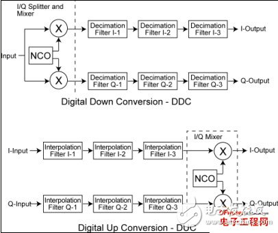
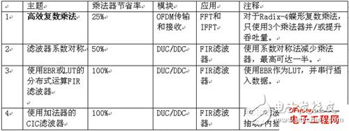
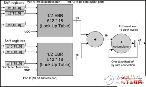
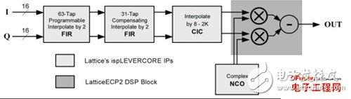
Emerging broadband wireless protocols based on WiMax and its derivative standards require higher and higher throughput and data rates. The fast chip rate and digital radio frequency processing proposed by these protocols can be best realized on hardware using FPGA solutions. FPGAs are very suitable as high-performance, cost-effective solutions to implement the digital functions in these physical layer protocols, because they include the following abundant resources: 1. DSP module, which can be used to realize the functions of multiplier and adder/accumulator required by various FIR filtering and FFT/IFFT operations; 2. SERDES transceiver, which can support CPRI and OBSAI interfaces between the wireless front end and the baseband digital board; 3. Important FPGA embedded RAM block memory (EBR), which can be used to store filter coefficients, perform block interleaving, and implement FEC decoding (Turbo, Viterbi, Reed-Solomon, etc.); 4. High-speed LVDS I/O supports wide parallel interfaces to DAC and ADC respectively. These converters define the boundary between RF/analog functions and inexpensive digital baseband logic. The higher the speed of the interface, the more digital up-conversion/digital down-conversion functions can be integrated in a low-cost FPGA solution. This article focuses on the first resource, the DSP multiplication module. By reducing and optimizing the implementation of DSP multiplication modules in FFT and FIR, designers can meet throughput requirements while minimizing resource usage, allowing users to use the most cost-effective off-the-shelf FPGA devices. These four multiplier saving techniques are introduced below. An important feature of WiMax system design is to support Orthogonal Frequency Division Multiplexing (OFDM). FPGA makes it particularly easy to implement OFDM transmitter and receiver in discrete time using IFFT and FFT, respectively. Protocols such as 802.16a require 256 samples of FFT. These 802.16e protocols require multiple FFT samples, or FFT samples that can be flexibly adjusted to adapt to dynamic channel and bandwidth requirements (scalable OFDMA). When performing 256 and 1024 sample FFT, the most efficient use of the multiplier can be obtained through the Radix-4 structure. The FFT algorithm decomposes by multiplexing the 4-point discrete Fourier transform (DFT) butterfly structure. For example, a 16-point FFT can be implemented with 2-level Radix-4 DFT structure by decimating by time, decimating by frequency or other relevant decomposition methods. The first level is composed of 4 4-point DFTs, and the second level is also composed of 4 4-point DFTs. Since the output of each DFT requires 3 phase factors for the result before being fed to the next stage, the 9 phase factors between the first and second stages require 9 complex multiplications. At first glance, performing a complex multiplication requires 4 multipliers and 2 adder/subtractors. However, this expression can be rewritten as another expression that only requires 3 multipliers, 3 adders, and 2 subtractors. It is worth noting that the adder is implemented in the core logic of the FPGA, using a rich general programmable logic unit (PLC) chip in the ripple mode. If D=Dr+jDi is complex number data and C=Cr+jCi is a complex number coefficient, then the standard expression of complex number multiplication is as follows: E1: R=D*C=(Dr+jDi)*(Cr+jCi)=Rr+jRi (1) Among them Rr=Dr*Crï¼Di*Ci, Ri=Dr*Ci+Di*Cr The above standard expression requires the use of 4 multipliers. The expression can be rearranged algebraically as: E2: Rr=Dr*Cr-Di*Ci (2) E3: Rr=Dr*Crï¼Di*Ci+0 (3) E4: Rr=Dr*Crï¼Di*Ci+(Dr*Ciï¼Di*Cr)ï¼(Dr*Ciï¼Di*Cr) (4) E5: Rr=(Dr*Crï¼Dr*Ci+Di*Crï¼Di*Ci)+(Dr*Ciï¼Di*Cr) (5) The new expression for the result of a complex number is: E6: Rrï¼[(Dr+Di)*(Crï¼Ci)]+(Dr*Ciï¼Di*Cr) (3 times multiplication) (6) E7: Ri=Dr*Ci+Di*Cr (multiplexing the product from Rr) (7) As shown in Figure 1, the optimal complex multiplication can be implemented with 3 multipliers, 3 adders, and 2 subtractors. It is worth noting that in FPGA, the relative die area used by the addition/subtraction module is smaller than the 18×18 multiplier module. Figure 1: Complex number multiplication with 4 and 3 multipliers. In short, a 25% reduction in the number of multipliers used can bring one of the following two major benefits: 1. Under the condition of the same FFT throughput, multipliers can be used less; 2. FFT throughput can be improved under the condition of the same number of multipliers. High-efficiency realization of FIR filter in digital upconverter/downconverter The following three high-efficiency multiplier techniques can be used to implement digital up-conversion and down-conversion in FPGAs. This has become a focus area for optimization, because wireless designers need to meet the requirements of transferring data from very high sampling rates to chip processing rates. The digital down-converter/up-converter (DDC/DUC) subsystem is the main digital device of the transmitter/receiver in the base station, which was previously implemented with expensive analog/mixed signal devices. There are three techniques that can be used to reduce the number of multipliers in an FPGA implementation. 1. FIR filters with symmetrical coefficients can save multipliers; 2. Distributed computing operations use embedded block memory; 3. The cascaded integrating comb filter uses an adder. As described in the upper part of Figure 2, DDC consists of the following components: an I/Q splitter based on a numerically controlled oscillator (NCO), which uses two mixers to use sine and cosine for the input signal from the RF part The wave is modulated; a decimation part can be configured by a 3-stage FIR decimation filter or an FIR decimation filter followed by a cascaded integrator comb (CIC) filter. Figure 2: DDC/DUC structure. The DUC in Figure 2 consists of the following components: a 3-stage FIR interpolation filter or a CIC filter followed by a FIR interpolation filter; an I/Q mixer based on NCO and two mixers. , Q output signals are demodulated before reaching the RF part. Remember that decimation is used for sample deletion to achieve a lower sampling rate, while interpolation is used to increase the extrapolated samples to increase the sampling rate. The DDC/DUC system is a system that requires a large number of multipliers. The decimation and interpolation filters are usually implemented by multipliers and adder arrays, and the mixing function is a multiplier. The realization of NCO using the area optimization method is based on the phase shift using a complex multiplier. Overcoming the challenges of systems that require a large number of multipliers is to decompose and cascade the filters first: 1. A large FIR decimation filter or FIR interpolation filter with a decimation/interpolation coefficient of N can be decomposed into two or three smaller and simpler stages with decimation/interpolation coefficients N1, N2, and N3. Coupled filter. The decimation/interpolation coefficient satisfies the following equation: E8: N=N1*N2*N3 2. Decomposing the FIR decimation filter or FIR interpolation filter into two or three independent filters can reduce the total number of taps required to implement the entire filter. A single filter with a decimation or interpolation coefficient of N requires a large number of taps (multipliers) to meet the basic filter attenuation and noise characteristics. Breaking the filter into two or three smaller and simpler filters can reduce the number of taps in the entire filter system. In addition, the lower sampling rate of the second and third cascade filters can achieve time multiplexing, thereby further reducing the size of the implementation. After the filter order is determined, a variety of measures can be taken to reduce the number of multipliers in the actual filter. This will be described below. Table 1: Four technologies that can reduce the number of multipliers in WiMax system design. 1. Symmetrical decimation and interpolation filters DDC decimation filters and DUC interpolation filters with symmetrical coefficients can be used to achieve a multiplier saving effect of up to 50%. Under the symmetric condition, the FIR filter coefficients h(0), h(1),..., h(n) of n taps satisfy h(k)=h(n-k) {0≤k≤n}. Since h(k)=h(n-k), the product of h(k) and the sum of two related samples can be completed at one time, so the number of multipliers required can be reduced by up to 2 times (for an even number of coefficients). In FPGA, low-cost bitwise carry logic can be used to implement the addition of two data samples using the same coefficient. 2. Realize FIR filter through distributed computing function and use EBR memory block For multiplier-intensive applications (such as DDC or DUC), the efficient use of FPGA resources is particularly important. Using memory and LUT structure resources as a multiplier can significantly improve implementation efficiency. EBR and distributed memory of this structure can be used as an FIR filter multiplier using distributed memory technology. Distributed memory technology is also called soft multiplication technology, using this technology can usually increase the number of multipliers in FPGA devices by 2 to 5 times. It can be seen from Figure 3 how to use EBR to implement an FIR filter using distributed arithmetic technology. The samples are serially shifted into the EBR address bus. Inside the EBR there is a pre-calculated result multiplication table and the sum of each input sample bit (address bit) with appropriate coefficients. The accumulator will accumulate n (n is the sample bit resolution) intermediate results and provide a complete FIR filtering result after n clock cycles. Figure 3: Using block memory as FIR multiplier. Replacing some parts of the interpolation/decimation FIR filter chain with CIC multipliers is another way to reduce the number of multipliers required for implementation. Is the CIC multiplier? ? /Down conversion usually requires a wide range of speed changes of hundreds of orders. High-rate varying interpolation or decimation filters are very expensive in terms of hardware. CIC filters are also known as Hogenauer filters and can be used as low-cost high-factor decimation or interpolation filters. They can be used to achieve arbitrary and large rate changes in digital systems, and can be efficiently implemented using only adders and subtractors. Because FPGA has a fast carry chain for implementing adders, CIC filters are very suitable for FPGA implementation. See Table 2 for the structure and characteristics of the integrator and comb filter. Table 2: The structure and characteristics of the comb filter and integrator. It is quite simple to implement DDC or DUC inverter with Lattice's FPGA, because FPGA provides important components used as IP core. The application of CIC filters as interpolators in data rate conversion is shown in Figure 4, which shows the use of CIC interpolators as frequency converters in digital wireless applications. Figure 4: Digital up-converter for digital radio applications. The digital upconverter uses the following IP core configurations: 1. FIR filter (interpolation filter with 63 taps); 2. FIR filter (interpolation filter with 31 taps); 3. CIC filter (interpolating CIC filter with a programmable rate between 8 and 2K); 4. NCO (NCO with sine and cosine output). The LatTIceECP2/M series of low-cost FPGAs have a variety of high-performance features that are highly relevant to WiMax system design. It is difficult to find these features in other low-cost FPGA series devices, but can only be found in expensive high-end FPGA products: 1. High-performance DSP module with hard-wired multiplier, adder/accumulator module and pipeline level; 2. SERDES transceiver channel with a rate of up to 3.125Gbps, supporting CPRI and OBSAI interfaces between the radio head and the baseband digital board; 3. A large number of 18kB EBR memory blocks in the LatTIceECP2/M memory enhancement series products; 4. Support high-speed LVDS I/O with ADC/DAC interface, input and output rates can be as high as 840Mbps; 5. Low-cost LatTIceECP2/M series devices can provide these rich and high-performance resources, and the price is much lower than other FPGA devices. WiMax system designers can also use a variety of design techniques to reduce the number of DSP multipliers required, allowing users to use smaller and cheaper FPGA devices. Jiangsu Stark New Energy Co.,ltd was founded in 2018. It is an emerging new energy manufacturer and trader. We produce high-quality lithium iron phosphate battery packs, including 12.8V100AH 25.6V100AH 51.2V50AH 100AH 200AH, etc., also 192V 384V and other high-voltage lithium batteries for Energy Storage System, as well as customized container energy storage system, the battery is currently compatible with inverters of all mainstream brands Battery Lithium Ion,Lithium Ion Battery 24V 100Ah,48V100Ah Lithium Ion Battery,Lithium Iron Phosphate Battery Jiangsu Stark New Energy Co.,Ltd , https://www.stark-newenergy.com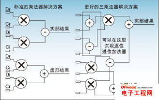
Matching communications, such as Growatt, Goodwe, Voltronic, Victron, SMA, Sungrow, Kehua, etc. The company is committed to the production,R&D and sales of lithium batteries and energy storage systems, aiming to provide customers with more cost-effective and more durable products , Our current lithium battery products
Mainly used in home solar power system, commercial energy storage system, uninterruptible power supply, etc., which are welcomed by overseas customers.

