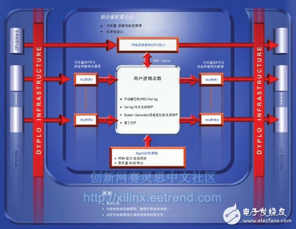
Over the past three decades, FPGA technology has evolved from a programmable logic array with a small number of registers to the advanced integrated system devices we see today. About a decade ago, major vendors began using 8-bit, 16-bit, and 32-bit soft-core processors in their FPGA devices for the first time to improve integration and functionality between processing and programmable logic. They then began to implement hardened versions of these processors, giving customers more system advantages. Xilinx's Zynq®-7000 All Programmable SoC is one of the best in this class. The Zynq SoC integrates the ARM® dual-core CortexTM-A9 MPCore processing system, FPGA fabric and peripherals in a single device, enabling software/hardware to achieve an unprecedented tight connection, bringing system-level integration and functionality to a whole new level. But this tighter integration also blurs the boundaries between hardware and software design because it introduces FPGA design into the software world and introduces application development into the FPGA space. The IP modules developed by our TOPIC Embedded Systems company significantly reduce the time and cost of system development on the Zynq SoC. The middleware of the Dyplo system can effectively bridge the gap between hardware and software design and help implement a complete software-based development process. Dyplo has automatic partial reconfiguration. This is an advanced design technique that instantly modifies the hardware configuration of the FPGA layout to give the FPGA the best performance for a specific application. Users can use graphical tools to drag features to individual partitions and then determine if they are performing optimally on the logic or processor. DYPLO: Dynamic Process Loader The principles of Dyplo can best be explained from a development perspective. When starting a design project, you must first determine the design requirements and define the customer requirements as abstract terms. At this stage, modifying the design requirements will not cause much impact. Next you need to translate the design requirements into design specifications, and at this point you need to develop a blueprint for the architecture. In this architecture development process, you need to determine which features should be implemented in hardware and set in time. In many cases there are multiple architectures to choose from, but due to budgetary and time constraints, it is usually only possible to study one architecture (or two if you are lucky). Modifying design requirements at this stage will result in significant cost loss. Once the architecture definition is complete, it's time to start designing various features. In the design process, you will often find some omissions, that is, you need to exchange content between hardware and software. This kind of interchange usually increases the amount of development work, because you have to start solving the problem of the groundbreaking control functions in the DSP type data flow that were not originally related to these related fields. As customers understand the complexity of design, their insights are growing, so this situation becomes quite common. Therefore, designers need an effective mechanism to exchange functions between hardware and software. Figure 1 shows a common arbitrary scheduling scenario for mapping processes to FPGA hardware and software. Figure (a) does not use a general allocation scheme. Therefore, a more structured and predictable infrastructure needs to be built between software and hardware. Dyplo implements this infrastructure, as shown in Figure (b). Figure 1 – (a) There are two separate processes in the diagram where the hardware designer enters the HDL into the logic module of the Zynq SOC and the software designer enters the software into the processor. In contrast, Dyplo creates a unified code entry point for hardware and software functions, as shown in (b), which facilitates system-level collaborative design and verification in a Linux environment. Dyplo provides users with a data stream interface for connecting hardware and software processes. It can take the communication between software processes, the communication between hardware processes, or the hybrid communication of software and hardware processes. You can use Dyplo to define hardware flows within reconfigurable partitions. To implement a given hardware function, you need to activate it on a reconfigurable partition, then initialize the input and output data streams to that partition and connect those data streams to software processes or other hardware processes. In addition to synchronizing data streams, you can synchronize processes such as frame boundaries, discrete sample moments, and software task alignment. The number of software processes depends on the operating system for which the design is designed and how the process communication is organized. The number of hardware flows depends on the number of reconfigurable partitions that are reserved on the FPGA. The number, size, and location of reconfigurable partitions can be either user-defined or automatically selected. Dyplo handles process communication and synchronization through a hardware and software communication backplane with scalable capabilities. For example, the default configuration allows four HDMI video streams to be active at the same time, while using the processor to maintain full data exchange. The Dyplo infrastructure, features mapped to reconfigurable partitions, and full Linux distribution generation are all implemented through a graphical tool flow that is compatible with the standard Vivado® Design Suite project flow. You can stop executing software and hardware processes immediately during the design process and continue after replacing the process functions. It is not important for the software process, the designer can enhance the code (only limited by the designer's functional limitations for the operating system selected by the project). For hardware processes, partial FPGA reconfiguration is required to replace the functionality of some FPGAs without affecting the execution of other programmable logic or external physical interfaces. At the same time, the logic module is automatically loaded and verified automatically. In this way, Dyplo integrates the execution of hardware processes in the software environment while providing software programmers with the functional advantages of FPGAs seamlessly. The Zynq SoC offers many advantages in hardware system level integration. All features are available for a fully software programmable platform. However, from an application perspective, a middleware is needed to achieve this architectural advantage. This is where Dyplo works. Leverage the value of partial reconfiguration Dyplo provides integrated partial reconfiguration support directly available. The default region of the reconfigurable partition is preserved based on configuration parameters such as the number of partitions required and the logical complexity of the reconfigurable partition. Dyplo automatically generates partial bit files after providing HDL functional descriptions such as reconfigurable modules. As part of the software application, the reconfigurable module acquires functionality by issuing simple software instructions. Dyplo is responsible for all the steps required to perform hardware functions, such as terminating the currently executing function, writing new functions, data flow connections, module configuration, and function activation. Benefits for Hardware Engineers What advantages can the integrated Dyplo architecture bring to FPGA design engineers? It makes design work easier by integrating with the processor environment while minimizing the underlying software support requirements. This means you can focus on design features. The advantages of FPGAs are particularly evident in applications such as high-speed interface design, high data bandwidth circuits, and accelerated algorithm processing. Designing interfaces and high-bandwidth circuits requires manual involvement and requires a deep understanding of the technical advantages of FPGA devices. For accelerated algorithm processing applications, system-level synthesis tools such as Vivado HLS will play an increasingly important role. However, when using high-level synthesis, you need to have some design experience to ensure the results. With the Dyplo infrastructure, it is easy to embed an algorithm processing module, which provides a high-speed configurable inter-process communication network for communication between algorithm processing modules, I/O modules, and processor execution functions. These processing modules are carefully architected and are ideal for partial reconfiguration. The module has a clear interface, such as a stream data interface that conforms to the AXI4 interface standard. It uses a high-speed interconnect structure and a simplified processor bus to connect directly to the processing system. Links to other FPGA logic or device I/O are implemented through dedicated, extensible interfaces. Dyplo's performance is sufficient to support multiple 1080p input and output video streams, and video stream connections can be achieved with a simple configuration. Advantages of FPGAs for Software Engineers Design teams can significantly simplify HDL coding with Dyplo, and gain more advantages in system software design. Dyplo enables design teams to separate software functions during hardware implementation, prototype them in software, convert them to hardware, and maintain the same interface behavior. In turn, different functions can share the same FPGA architecture under software control. This solution requires smaller devices and lowers FPGA costs, which is comparable to software threads. From a software system perspective, the correlation between a single process and a connection can be thought of as a process network with data and event synchronization mechanisms. Figure 2 shows how software and hardware processes relate to the Dyplo infrastructure. Figure 2 – Spheres, Squares, and Pyramids represent functions or processes that can run in FPGA hardware or software. Each process is sealed in a Dyplo cover (a box around the figure). The arrows represent the flow of data from the input to the output through different processes. The Dyplo interface is responsible for managing the entire process. This approach also provides dynamic performance scaling because multiple instances of the same functionality can be implemented based on the system execution environment. The result is a more flexible and GPU-accelerated process execution. This technology also allows FPGAs to be used more by software engineers because interface protocols are simpler and can break complex designs into multiple modules that are more complex and controllable. More importantly, Dyplo and Vivado HLS are perfectly matched due to interface compatibility, which is ideal for software-based development processes. Testing with Dyplo is also easier. The flow of data to and from the HDL module is stored in a file used by the HDL test platform to generate patterns. This means that the development team can focus on testing the required features during the verification process. Complex system integration in test and debug environments is time consuming and more difficult to verify. After we developed the Dyplo infrastructure, we all know that design testing and integration work takes up most of the development time and is the most tedious part of the development process. During the configuration process, the underlying Dyplo environment generates the testbench templates used for validation. For example, the Dyplo environment generates a functional testbench template for each reconfigurable module in the architecture, implementing stream input and output of files or regular expressions, and a bus function model for implementing the CPU interface (see Figure 3). This way, designers can adopt a test-based design approach. This infrastructure allows the design team to step through the design to identify problems and perform backplane performance analysis to visualize all relevant state information in the fabric. The concept is so flexible that stopping the HDL logic of the Dyplo infrastructure will automatically synchronize software execution. This feature is key to identifying and resolving interfaces and dynamic issues. Figure 3 – Data flow input and output using a functional test template, while the CPU interface is implemented by the bus function model. Filling the gap TOPIC Embedded Systems, based in the Netherlands, has been developing embedded systems for many years, and the projects involved are usually integrated with various types of FPGAs and processors. Over time, we have become an expert in advanced FPGA design techniques, including partial reconfiguration. As a multi-core platform with embedded FPGA technology, Zynq SoC can significantly improve the efficiency of embedded system design. But the challenge for many design teams is how to get the most out of the Zynq SoC rich feature set based on the technical expertise of hardware and software engineers. Our Dyplo middleware can fill this gap. GPU-oriented applications can be implemented on an FPGA fabric with the same amount of work and greater flexibility. Making full use of reconfiguration technology makes the reuse of FPGA architecture simple from a software application perspective and helps reduce product costs. Automating many underlying design, integration, and testing tasks during FPGA design and software design can simplify the design process. In short, the productivity, flexibility, and performance optimizations enabled by the Dyplo middleware system help design teams bring the Zynq SoC's performance to the utmost and bring innovative system designs to market faster. A trial version (beta version) for qualified users will be available on December 1, 2013. If you would like to participate in a trial project, please contact us. The commercial version will be available on March 1, 2014. Lcd Bar Display,Shelf Edge Display,Stretched Bar Lcd,Stretched Bar Display APIO ELECTRONIC CO.,LTD , https://www.displayapio.com
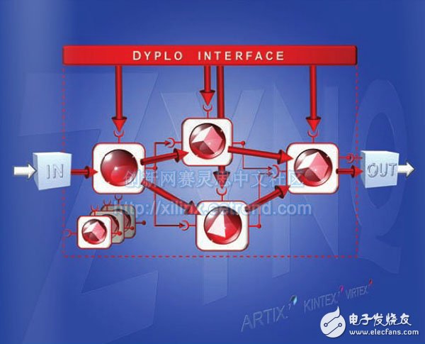
Dyplo is a middleware IP module. The module connects the scalable data flow between each FPGA process and the software flow executed by the processor through a standard AXI interface. 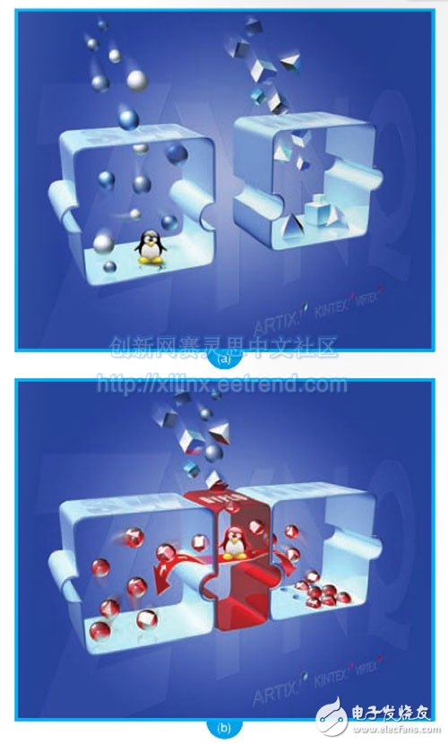
Dyplo takes full advantage of the partial reconfiguration capabilities of FPGAs. Partial reconfiguration is not a trivial task for designers because of the high complexity of loading and managing portions of the bitstream file and the need to maintain design continuity when changing PFGA components. In addition, the placement and routing of physical components requires considerable FPGA design experience.