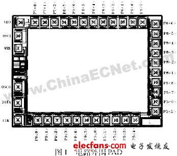
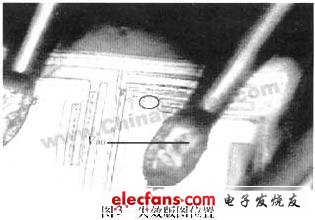
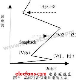
1 Introduction The effective design of ESD (Electric StaTIc Discharge) protection structure is one of the important tasks of CMOS integrated circuit reliability design. Its ESD structure is closely related to process technology and feature size. With the further development of IC process technology, the feature size is more and more Small, the thickness of the gate oxide layer of the tube is getting thinner and thinner, the area of ​​the chip is getting larger and larger, and the surrounding environment has not changed. Therefore, the failure of ESD is facing more and more severe tests, in submicron CMOS ICs. Usually, LDD (Lightly-Doped Drain) injection is used. In deep sub-micron ultra-large-scale CMOS IC design, there are usually Silicide or Salicide technologies. The use of these technologies helps to improve the speed, integration, reliability, etc. of the circuit, but These techniques are extremely detrimental to the ESD performance of the circuit, reducing ESD reliability. In sub-micron circuit design, the full-chip ESD protection structure of the circuit needs to be designed. How to make the full chip effective area as small as possible, ESD performance reliability meets the requirements and no need to add additional process steps becomes a major consideration for full chip designers. 2 circuit example The circuit is a keyboard coding control circuit, adopting 0.5μm-0.6μm SPSM CMOS well process, working voltage is 3V, 5V, integration degree is about 5000 gates except ROM, area is 2.0 &TImes; 1.5mm2, a total of 39 PAD, of which I 36 / O pins, one clock oscillating input pin, one VDD, one VSS. The PAD arrangement is shown in Figure 1. The protection structure of the I/O port is a Finger type MOS output tube and a GGNMOS tube, and there is a VDD-VSS voltage clamp protection circuit beside VDD and VSSPAD, and the logic structure is shown in FIG. 2. When the circuit is normally powered up, the N1 tube acts as a reverse diode between VDD and VSS, and when ESD occurs, the N1 tube turns on, as an ESD transient low impedance large current bleeder channel, between VDD and VSS. The voltage is clamped to protect the internal circuitry. This structure is also known as an ESD transient detection voltage circuit, where R is composed of an N-well resistor and C is a MOS capacitor. The ESD strike test was performed using the human body model industrial test standard HBMMIL-STD-883C method 3015.7, one of the ESD models. As a result, the I/O-VDD, I/O-VSS, and I/OI/O modes can reach more than 4kV, but in VDD-VSS mode, they can only reach 750V. At 1kV, the power supply and ground. A short circuit causes the entire circuit to fail. The preliminary analysis results show that the protection structure between the power supply and the ground is shown in Figure 2. There is a weak link in the design of the layout, which makes the structure's own robustness level, thus affecting the ESD performance of the entire circuit. In order to verify this idea and find an improved way, the following experiment was performed on the circuit. First, do a liquid crystal analysis experiment on the circuit, that is, drop a few drops of special chemicals (having fluidity) on the circuit, and then inject a large current into the VDD and VSS pins. The chemical liquid collects on the VDD and VSS paths. The current is concentrated at the point where the breakdown point is found. The breakdown point is near VDDPAD, as shown in Figure 3. Then, the FIB experiment was further carried out on the circuit, that is, the structure in the circuit was removed by laser, and then the ESD strike experiment was performed. The ESD result showed that the ESD strike voltage exceeded VDD-VSS mode, and the ISD resistance voltage exceeded 5 kV, but I/O-VDD, In the I/O-VSS and I/OI/O modes, the worst case can only reach 1.3kV, and the short circuit fails. Therefore, from the ESD experimental results of this circuit and the experimental analysis done, we can get: (1) In the circuit, the VDD-VSS voltage clamp protection structure is necessary to improve the ESD performance of the entire circuit and cannot be easily removed. (2) The structure itself must have a certain degree of robustness, so the design dimensions and layout design rules of each device in the structure are very important. The effective design of the VDD-VSS voltage clamp structure in the design of sub-micron CMOS IC ESD structures will be further explored below. In the HBM (Human Body Model) model, there are mainly three ESD strike schemes: (1) I/O-VDD/VSS; (2) I/OI/O; (3) VDD-VSS; Several methods are relatively independent and affect each other. In I/O-VDD/VSS mode, the direct protection structure of VDD and VSS is mainly used for each I/O port, which is usually placed on both sides of each I/O PAD, such as For simple diodes, Finger type GGNMOS (Gate-Ground NMOS), TFO (Thick-Field-Oxide) field tube, SCR or a combination of several structures, etc., mainly use the Snap back-down of the transistor to snap back the voltage in the collapse region. Clamping, see Figure 4, where the circuit is susceptible to damage in PS-mode and ND-mode modes; I/OI/O and VDD-VSS modes are directly ESD-protected devices between VDD and VSS and full-chip ESD The design of the protective structure is extremely relevant. In particular, the design of the ESD low-impedance and high-current bleeder channel, which is directly effective between the whole chip VDD and VSS, can effectively improve the overall ESD resistance of the circuit. The ESD structure design of the whole chip will be briefly explained at the end of the article.
Speakers are one of the most common output devices used with computer systems. Some speakers are designed to work
specifically with computers, while others can be hooked up to any type
of sound system. Regardless of their design, the purpose of speakers is
to produce audio output that can be heard by the listener.
Speakers are transducers that convert electromagnetic waves into sound waves. The speakers receive audio input from a device such as a computer or an audio receiver. This input may be either in analog or digital form. Analog speakers simply amplify the analog electromagnetic waves
into sound waves. Since sound waves are produced in analog form,
digital speakers must first convert the digital input to an analog
signal, then generate the sound waves.
The sound produced by speakers is defined by frequency and amplitude.
The frequency determines how high or low the pitch of the sound is. For
example, a soprano singer's voice produces high frequency sound waves,
while a bass guitar or kick drum generates sounds in the low frequency
range. A speaker system's ability to accurately reproduce sound
frequencies is a good indicator of how clear the audio will be. Many
speakers include multiple speaker cones for different frequency ranges,
which helps produce more accurate sounds for each range. Two-way
speakers typically have a tweeter and a mid-range speaker, while
three-way speakers have a tweeter, mid-range speaker, and subwoofer.
Speaker System,Magnet Speaker Acoustic,Moving Coil Loudspeaker,Metal Frame Mylar Speaker Jiangsu Huawha Electronices Co.,Ltd , https://www.hnbuzzer.com