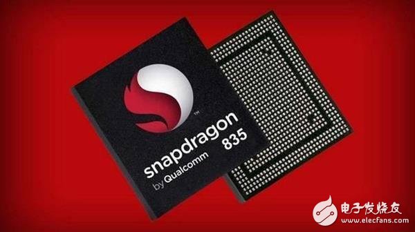
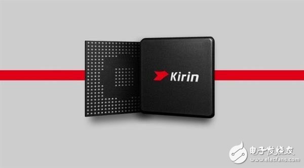
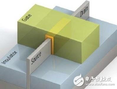
With the development of smart phones, the semiconductor technology has also rapidly increased. From 28nm, 16nm, 10nm to 7nm, these semiconductor foundries are rushing to release the latest technological processes every day, so that many people who eat melons are so eager to know that they are useful. The semiconductor industry seems to be far away from us. What is FinFET and what new technology is EUV? Every time I see this kind of related news, it makes us feel like a cloud. In fact, it is very close to us, whether it is FinFET or EUV is to make efforts to improve the process technology. The performance, heat dissipation, power consumption, etc. of a processor are closely related to the process. Today, let's talk about these things about the phone processor. ◠16nm, 10nm, what are these numbers? Speaking of this topic, we must first figure out what is the process. What are those 20nm and 16nm? In fact, these values ​​represent one thing, that is, the etching size of the processor. Simply put, we can engrave a unit of the transistor on a chip of a large size. The mobile phone processor is different from the general computer processor, and the size that can be left in a mobile phone is quite limited. The smaller the etch size, the more computing units are available in the same size processor and the better the performance. This is why manufacturers often emphasize processor processes. At the same time, as the frequency increases, the heat generated by the processor increases, and another important advantage of the more advanced etching technology is that it can reduce the resistance between the transistors, so that the voltage required by the CPU is reduced, thus driving them. The power required is also greatly reduced. Therefore, each new generation of products is not only a significant increase in performance, but also a reduction in power consumption and heat generation. In summary, it can be found that the processor's process is very important for mobile phones, higher performance brings a smoother gaming experience, and a body that maintains normal temperature can guarantee a good user experience. The upgrade of one process brings double improvement of heat dissipation and calculation performance. Regardless of the electronics, the CPU is a core component. ◠The development and performance of mobile phone processes are always together So today, the performance of mobile phones continues to improve, the semiconductor industry has contributed. From the 32nm Exynos 4412 to the current 10nm Exynos 8895, it has been less than five years, but the performance of mobile phones has increased by a factor of two. The increase in screen resolution and the increase in lens pixels are all closely related to the performance of mobile phones. Only with higher computing speed support, can we support larger resolution image output and stronger camera algorithms. Most of the current mobile phone processors are handed over to two manufacturers. In addition to TSMC mentioned above, there is Samsung. Both of them have been chasing you up and not relaxing. Samsung just launched the 32nm process, and TSMC is chasing after the 28nm new process. Here I just took out the 16nm solution, and I announced that 14nm is about to be put into commercial use. Without competition, there is no development. It is precisely because of the constant competition between the two families that the mobile phone industry can not fall into the ascending rhythm of “squeezing toothpaste†like a computer processor. This is not, how long our 10nm chip has not been used, Samsung's 8nm, TSMC's 7nm has been vying for release. Snapdragon 835 with the latest 10nm technology ◠Under the process, there are actually more games. Having said that, is the processor's process really so important? Take Apple as an example. Why did Apple, which had always chosen Samsung as its own processor foundry, chose TSMC's 16nm process on iPhone 7/Plus and gave up Samsung's 14nm? Technology is naturally because the process of TSMC on the 16/14nm process is more mature and perfect. At the beginning of the two versions of the A9 processor, Apple chose Samsung and TSMC to produce a version of each of them, and TSMC is slightly stronger than Samsung's performance, and it is one of the reasons why Apple completely reversed TSMC on the iPhone 7. But in addition to the process, in fact, manufacturers need to consider more. The Helio X30 is the next-generation flagship processor released by MediaTek at the MWC at the beginning of the year, and it took the lead in using the 10nm process before Samsung Qualcomm. Unfortunately, the yield rate of the new production process in the early stage is not ideal, and now TSMC has to fully open the order for Apple's A11 order. The X30, which is also manufactured by it, will inevitably have insufficient capacity. This chip, which has been highly anticipated by MediaTek, has not yet been seen. It is rumored that Huawei's Kirin series processors will soon release new products. ◠5nm, 3nm, or simply quantum calculation? In fact, the size of semiconductor etching has been difficult to develop. The size of each atom is about 0.1 nm. In the case of 10 nm, a line has less than 100 atoms, which is quite difficult to fabricate, and as long as there is an atomic defect, For example, if there are atoms falling out or impurities in the production process, it will cause unknown phenomena due to quantum effects, which will affect the yield of the product. FinFET technology concept map In fact, we have already encountered the bottleneck of the process. At the beginning, we converted the planar structure of the transistor into a three-dimensional structure, that is, the use of FinFET (Fin Field Effect Transistor). We broke through and ushered in the era of 10nm process. From 10nm onwards, the development of the processor is based on the new etching process, Extreme Ultraviolet Lithography (EUV), which uses a smaller and sharper "scalpel" to cut a smaller transistor structure. At present, it seems that Apple's next-generation product A11 will still be a 10nm process, so who will be the first to bring a newer and better process technology, is TSMC's 7nm or Samsung's 8nm, who will be the first processor Home? We will wait and see. Tension insulator,Double Tension Insulator String,High Tensile Wire Insulators,Metal end fittings TAIZHOU HUADONG INSULATED MATERIAL CO.,LTD , https://www.thim-insulator.com