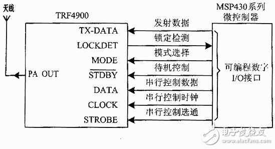
The wireless digital transmitting circuit uses a wireless transmitting chip TRF4900. The TRF4900 is a monolithically integrated, low-cost, fully functional multi-channel FSK transmitter from TI. The chip can meet linear (FM) or digital (FSK) emissions applications in the 868 MHz band in Europe and the 915 MHz ISM band in North America. The monolithic transmitter chip operates from 2.2 to 3.6 V with a typical transmit power of 7 dBm and low power consumption. The 24-bit direct digital synthesizer has an 11-bit DAC, and the synthesizer has approximately 230 Hz of channel space, allowing for narrowband and wideband applications. Two fully programmable modes of operation - Mode 0 and Mode 1, allow very fast transitions between two pre-programmed settings (eg transmit frequency 0 or transmit frequency 1). An on-chip integrated voltage-controlled oscillator (VCO), phase-locked loop (PLL), and reference oscillator require only a few external components to form a complete transmit circuit. The TRF4900 is connected to the TI MSP430 microcontroller via a serial interface. Each function block of the transmitter is capable of programming its functions via a serial interface. The TRF4900 is connected to TI's MSP430 microcontroller via a serial interface as shown. Circuit principle: TRF4900 pin 23 (LOCKDET), PLL phase lock detection output, effective high level. When LOCKDET = 1, the PLL is locked. Pin 11 (MODE), mode select input, device function in mode 0 and mode 1 can be programmed through the A, B, C, D word of the serial control interface. Pin 12, sleep control, active low. The contents of the control registers are still valid and can be programmed via the serial control interface. Pin 14 (TX-DATA), digital modulation input, FSK/FM modulation for carrier, active high. The serial control interface is a 3-wire unidirectional serial bus (CLOCK serial interface clock signal, DATA serial interface data signal, STROBE serial interface strobe signal) for programming the TRF4900. The registers inside the interface contain all user-programmable variables, including DDS frequency settings, as well as all control registers. The timing of the serial interface is shown in the figure. On each rising edge of the CLOCK signal, the logic value on the DATA pin is written to the 24-bit shift register. Set the STROBE terminal high and the programmed information is loaded into the selected latch. When the STROBE signal is high, the DATA and CLOCK lines must be low. Therefore, the signals of STROBE and CLOCK are not synchronized. The serial interface can be programmed to operate in an active or sleep state (standby mode). The wireless digital transmission circuit composed of TRF4900 and MSP430 can be easily embedded in various measurement and control systems; it can be applied in instrumentation data acquisition system, wireless meter reading system, wireless data communication system, computer telemetry remote control system and so on. The main features are wireless digital transmission circuit with low transmission power, stable circuit voltage reading, easy to set serial communication parameters, suitable working frequency bandwidth, and easy signal transmission through FSK modulation. Ev Charging Cable,Electric Car Charging Cable,Type 2 Charging Cable,32A Ev Charging Cable Yangzhou JERI New Energy Co., Ltd. , https://www.jrevcharging.com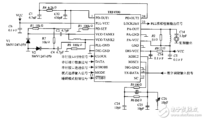
Electronic enthusiast network technology editors comment analysis:
If you have any questions, please feel free to discuss them in the comments section.
- Electronic enthusiast network finishing, please indicate the source!