2 Bandgap Reference Principle The bandgap reference outputs a stable DC voltage that is insensitive to temperature and supply voltage. Integrated circuits typically use standard voltages with opposite temperature coefficients and independent of supply voltage. These two standard voltages achieve inter-element matching and temperature tracking through mutual compensation. This article refers to the address: http:// In the circuit, a PNP constant current source composed of two identical transistors VP1 and VP2 can be used as a collector active load of the VN1 and VN2 transistors, a transistor VN2 provides a base-emitter voltage (UBE), and a voltage ΔUBE is generated on the resistor R1. . Since IE1=IE2, then: Bandgap reference circuit of FIG. 3 with a conventional operational amplifier 2 with operational amplifier is a bandgap reference circuit, an operational amplifier incorporated solve voltage instability. Since the circuit connection has a negative feedback, the VQ1 and VQ2 clamps are at the same potential, the power supply rejection ratio is increased, and the power consumption is lowered. However, its traditional bandgap reference circuit has problems such as the inherent offset of the operational amplifier. Amplifying the input offset voltage of the operational amplifier causes an error in the output voltage, which seriously affects the accuracy of the bandgap reference voltage source. At the same time, its input offset voltage varies with temperature. This increases the temperature coefficient of the output voltage. Therefore, the system design does not use an operational amplifier and also achieves better performance. A1, A2, and A3 are the emitter areas of the NPN transistors VN1, VN2, and VN3, respectively, and AA: A2: A3 = 1: P: Q (P and Q are constant), and the equation (1) shows: The first two terms of equation (7) are the current proportional to the absolute temperature (PTAT). With IPTAT, the conventional reference only uses this current to compensate UBE, and the improved circuit VN3, R3 can generate the nonlinear partial current INL, ie The last term of equation (7) can effectively compensate the nonlinear part of UBE to achieve better temperature characteristics, so: 5 Simulation results Using Cadence spectre to simulate the temperature sweep and power supply variation analysis of the circuit respectively, due to the error between the parameter calculation result and the simulation model, the simulation should be properly adjusted to ensure the normal output reference voltage. As shown in Figure 4, when the temperature changes from 50 °C to 150 °C, the UREF changes from 1.260 3 V to 1.265 2 V, the maximum variation is 4.9 mV, and the temperature coefficient is 24 ppm/°C. The temperature coefficient of the ordinary first-order compensated bandgap reference is greater than 30 ppm/°C, so the improved circuit performance is greatly improved. 6 Conclusion Based on the analysis of the traditional bandgap reference voltage source with operational amplifier, the curvature compensation technology is applied to design a bandgap reference voltage source suitable for vehicle electronics. The circuit adopts bipolar technology, and the structure is simple and novel. High and portable. The Cadence Spectre simulation results show that the circuit can stabilize the output over a wide temperature range, with a rate of change of only 24 ppm/°C with temperature, and the power supply is well suppressed. Strong anti-interference ability, fully in line with automotive electronics standards. Our company specializes in the production and sales of all kinds of terminals, copper terminals, nose wire ears, cold pressed terminals, copper joints, but also according to customer requirements for customization and production, our raw materials are produced and sold by ourselves, we have their own raw materials processing plant, high purity T2 copper, quality and quantity, come to me to order it! Cable Terminals Taixing Longyi Terminals Co.,Ltd. , https://www.longyicopperlugs.com
Bandgap reference voltage sources are widely used in A/D converters, D/A converters, integrated voltage regulators, and sensor interface circuits. With the large-scale circuit system and the development of SOC, the system design requires high temperature, voltage, process stability and circuit board area of ​​the bandgap reference voltage source. In particular, the automotive electronics industry places high demands on chip integration, power supply stability and security.
Based on the analysis of traditional reference voltage source and demonstration curvature compensation technology, a design scheme of bandgap reference voltage source circuit suitable for automotive ABS wheel speed sensor interface is proposed. Taking into account the environmental factors such as large temperature difference, noise, and poor road conditions during operation, the complicated operational amplifier is not used, and the first-order curvature compensation technology is used, which greatly improves the stability and anti-interference ability of the voltage source. The use of the proven Bipolar process can effectively reduce the damage rate of the device. The design also introduces a startup circuit that solves the problem of additional power consumption of the conventional bandgap reference voltage source. The circuit simulation was carried out using the Cadence Spectre tool. The results show that the design meets the requirements of automotive electronics and has high practical value.
Figure 1 shows a typical two-tube bandgap reference source circuit that uses the effective emitter junction area ratio of the VN1, VN2 tubes and the resistance ratio of the resistors R1, R2 to obtain a reference source close to zero temperature coefficient. 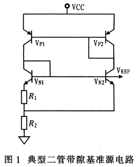
![]() Where: ΔUBE=Ut1n[(IEl/AE1)/(IE2/AE2)]=Utln(J1/J2); J is the current density, J=I/A; AEl and AE2 are the effective area of ​​the emitter junction.
Where: ΔUBE=Ut1n[(IEl/AE1)/(IE2/AE2)]=Utln(J1/J2); J is the current density, J=I/A; AEl and AE2 are the effective area of ​​the emitter junction.
Since IE1=IE2, J has nothing to do with temperature, so: ![]()
In theory, as long as R1, R2, AEl, and AE2 are properly set, the output can reach the ideal temperature coefficient. Due to the instability of the collector voltage of VP1 and VP2, the actual output deviates from the theoretical value. Therefore, the operational amplifier is introduced into the reference power supply. 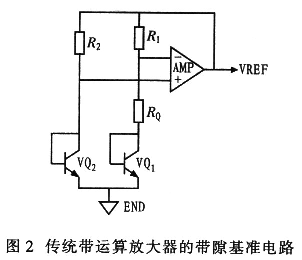
4 Design of bandgap reference based on automotive environment
4.1 Bandgap reference voltage source design using first-order curvature compensation technology Figure 3 is a bandgap reference voltage source circuit applied to automotive ABS wheel speed sensor interface. The circuit design uses bipolar process and first-order curvature compensation. The technology, considering the temperature variation of the vehicle driving environment, the limited space of the vehicle body and the safety performance, requires the circuit to have a wide temperature range, a small circuit area, a high power supply rejection ratio, and stable performance. 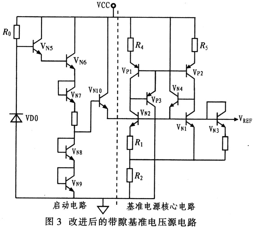
![]()
Where k is a Boltzmann constant, k=1.380x10⁻²³J/K; T is temperature; q is the electron charge; q=1.602x10⁻¹⁹C. 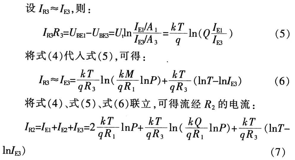

In the formula, n is a constant, which is related to the fabrication process of the transistor, n=1.5-2.2.
After the circuit is powered up, the BE junction diode of VN9 and VN8 can clamp the base of the NN10 to 1.4V. VN10 is turned on, and current is injected from VCC through VN10 into the bases of VN1, VN2, and VN3. These three transistors are turned on, thereby reducing the power consumption of the startup transistor. After the reference supply voltage is activated, the emitter level of VN10 is raised and VN10 is turned off.
4.2 Layout design Due to the particularity of the automotive environment, the layout of the circuit board is required to be strict. The overall circuit adopts the Shanghai Belling 2μm 40 V Bipolar process. Bipolar processes are much more stable than MOS processes, typically have lower breakdown and damage rates, and are more resistant to radiation and interference. In the layout, attention should be paid to noise interference and debugging accuracy. The bandgap reference should be placed close to the power supply and ground, and the ground should be set separately from the other modules. This avoids the ripple generated by the two grounds. Superimposed. Three small-sized test pads are connected to a plurality of resistors on both sides, and the output value of the actual device can be tested by blowing the wire between them, which provides convenience for accurate debugging of the device.
At 27 °C, when the power supply voltage (U) changes from 5 to 16 V, the UREF variation range is 1.264 60 to 1.264 97 V, and the variable is 0.37 mV. The power supply rejection characteristic curve of UREF is shown in Figure 5. . 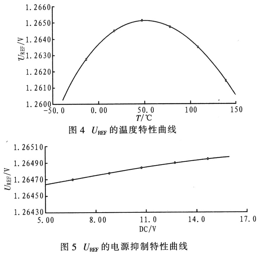
1 Introduction