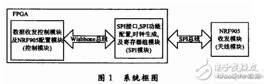
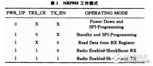
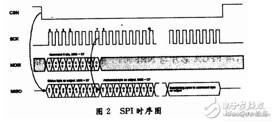
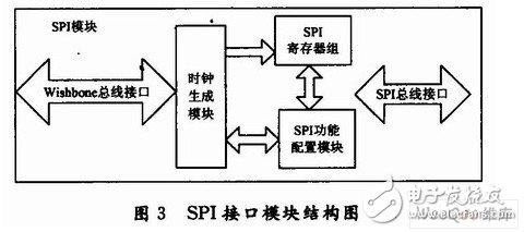
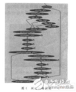
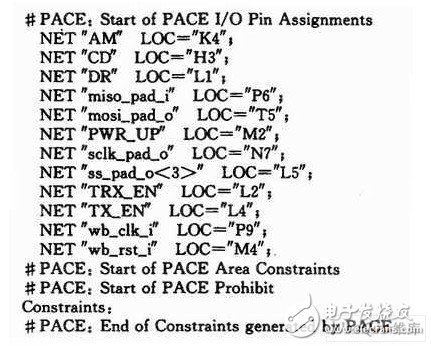
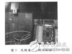
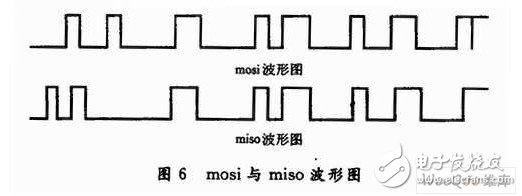
With the rapid development of computer technology, electronic information technology is becoming more and more popular in applications in all walks of life. The traditional way of collecting logistics information is to check the ticket by the staff, and then input the data on the ticket into the computer. This process is time-consuming and laborious, and may cause various kinds of erroneous data due to various human errors, which affects the reliability of the collected information. The automatic identification technology uses a computer for automatic identification, which increases the flexibility and accuracy of input, frees people from the complicated statistical identification work, and greatly improves the efficiency of logistics information collection. At present, RFID applications promoted by Wal-Mart, Metro and other large supermarkets have brought benefits to the retail industry, including reduced labor costs, improved product visibility, reduced losses due to product outages, and reduced product theft. The applicable process includes: real-time statistics of commodity sales data, replenishment, anti-theft, etc. This article uses RFID technology, builds a wireless communication system with FPGA chip and NRF905, and successfully realizes wireless sending and receiving of data. RFID (Radio Frequency IdentificaTIon, radio frequency identification technology) is the use of radio waves to read/write recording media. The distance of radio frequency identification can reach several tens of centimeters to several meters, and according to the read/write mode, thousands of bytes of information can be input, and at the same time, it has extremely high confidentiality. Application areas of RFID technology: material tracking, delivery vehicles and shelves It is especially suitable for occasions that require non-contact data collection and exchange, such as identification, and that require frequent changes in data content. For example, the automatic vehicle identification system in Hong Kong uses radio frequency technology as the main technology. Radio frequency technology has also been widely used in the automatic management of identification of other items. As shown in Figure 1, the entire architecture of the wireless system is composed of a control module, an SPI module and an antenna module. The configuration of the SPI module is completed by the control module through the Wishbone bus, and the configuration of the antenna module, mode conversion, and data transmission and reception are all completed by the control module through the SPI bus. Each part will be explained below. NRF905 is a monolithic radio frequency transmitter chip launched by Norway Nordic Company. The operating voltage is 1.9-3.6 V, 32-pin QFN package, and it works on three ISM channels of 433/868/915MHz. It can automatically complete the work of processing the prefix and CRC (cyclic redundancy check), and can automatically complete Manchester encoding/decoding by the on-chip hardware, using SPI interface to communicate with the microcontroller, easy to configure, low power consumption, with -10 dBm The current is only 11 mA when the output power is transmitted, and 12. 5 mA in the receiving mode. NRF905 has ShockBurst receiving and ShockBurst sending two working modes; power-down and SPI programming and Standby and SPI programming two power-saving modes. The characteristic of its ShoesBurst working mode is to automatically generate preamble and CRC, which can be programmed and configured through the SPI interface. The working mode of NRF905 is set by the setting of TRX_CE, TX_EN, PWR_UP, see Table 1. All configurations of nRF905 are carried out through SPI interface. The SPI interface is composed of 5 registers, and an SPI instruction is used to determine what operation to perform. The SPI interface is only active in power-down mode and Standby mode. The five registers of the SPI interface are: (1) Status register: The register contains data ready DR and address matching AM status. (2) RF configuration register: The register contains configuration information such as the frequency and output power of the transceiver. (3) Sending address: The register contains the address of the target device, and the byte length is set by the configuration register. (4) Send valid data: The register contains the sent valid Shock Burst packet data, and the byte length is set by the configuration register. (5) Receive valid data: The register contains the received valid ShockBurst packet data, and the byte length is set by the configuration register. The valid data in the register is indicated by the data ready DR. ShoekBurst technology enables nRF905 to provide high-speed data transmission without the need for high-speed controllers for data processing or clock coverage. By putting the high-speed signal processing related to the RF protocol into the chip, nRF905 provides an SPI interface to the application controller, and the rate is determined by the interface speed set by the microcontroller itself. nRF905 reduces the speed of the digital application part to reduce the average current consumption in the application when the RF is connected at the maximum speed through the ShockBurst working mode. In ShockBurst RX (receive) mode, the address matching AM and data ready DR signals inform the controller that a valid address and data packets have been received respectively. In ShockBurst TX (transmit) mode, nRF905 automatically generates the preamble and CRC check code, and the data is ready DR signal to notify the controller that the data transmission has been completed. The SPI (Serial Parallel Bus) bus is a synchronous serial peripheral interface proposed by Motorola, which allows the CPU to communicate with various peripheral interface devices in a serial manner. It uses 4 lines: serial clock line (SCK), master input/slave output line (MISO), master output/slave input line (MOSI), low-level active enable signal line (SS). In this way, only 3 to 4 data lines and control lines are needed to expand various I/0 devices with SPI interfaces. The data in the SPI bus mode is transmitted in bytes (multiple bytes can be transmitted in one transmission), each byte is 8 bits, and each command or data block is byte-aligned (8 clock integers) Times). Data is transmitted bit by bit, with high bit first and status second. It is full-duplex communication. The data transmission speed is generally faster than the I2C bus, and the speed can reach several megabits per second. The SPI interface works in a master-slave mode. This mode usually has a master device and one or more slave devices. In the wireless communication system designed in this article, the SPI bus interface module implemented by FPGA is the master, and the SPI module of NRF905 is the slave. Selection of SPI timing mode: The SPI interface has 4 different data transmission timings, which are a combination of CPOL and CPHL. CPOL is used to determine the level of the SCK clock signal when it is idle; CPOL=O, the idle level is low, and when CPOL=1, the idle level is high. CPHA is used to determine the sampling time, CPHA=0, sampling at the first clock edge of each cycle; CPHA=1, sampling at the second clock edge of each cycle. Figure 2 is the timing diagram of the SPI interface of NRF905, so the SPI working mode designed in this article is under this timing of CPOL=O, CPHA=O. Figure 3 is the structure diagram of the SPI module in the wireless communication system of this article. The SPI in the system is mainly composed of a clock generation module, an SPI register set, and a module for SPI function configuration, and is connected to the controller through the Wishbone bus. The specific design is as follows: Clock generation module: Because the SPI module is implemented based on FPGA, and the clock provided outside the FPGA is faster (50 MHz or 100 MHz), it is not suitable for communicating with the SPI interface of NRF905 (1 Hz~10 MHz), so it needs to be divided. To slow down the clock frequently. But as for the number of frequency divisions, it is done by the SPI function configuration module. Secondly, because the SPI protocol points out that the data can be triggered on the rising or falling edge, it is also necessary to identify the rising or falling edge of the clock (also called the edge grab procedure). This function is also completed by this module. SPI register module: This module implements a 128-bit register group composed of 16 8-bit registers, which means that 8-128-bit serial data can be sent and received at one time through the SPI interface. The specific operation is completed by the SPI function configuration module. SPI function configuration module: This module is equivalent to an SPI controller, which determines the frequency division of the clock, the number of data sent and received, and the data transmission on the rising or falling edge of the clock through the configuration of its registers. The configuration of these registers is Completed by the control module. The following is a brief description of the configuration registers. First introduce the control register: Bit 0 of the control register go: whether to start sending. The first bit of the control register rx_negedge: whether the received data is a falling edge or a rising edge. The second bit of the control register tx_negedge: whether the sending data is a falling edge or a rising edge. Bits 3 to 9 of the control register char_len: the number of digits of data sent (because SPI is full-duplex, this is actually the number of digits of received data). The 10th bit lsb of the control register: whether it is sent from the high position or the status. The 11th bit of the control register ie: whether to send an interrupt signal after the read and write is completed. The 12th bit of the control register ass: whether to automatically generate a chip select signal. Frequency divider register: spi_divider_sel. Status register: spi_ctrl_sel. Data register O: spi_tx_sel[0]. Data register 1: spi_tx_sel[1]. Data register 2: spi_tx_sel[2]. Data register 3: spi_tx_sel[3]. Chip select signal register: spi_ss_sel. For the control module, the implementation method is to use a finite state machine based on Verilog language, which is equivalent to one instruction to control the SPI module to receive and send data. The control module is divided into three independent parts, namely the receiving control module, the sending control module and the NRF905 configuration module. Among them, the receiving and sending control modules respectively include the status of configuring the SPI. The following describes the design of the receiving control module. Figure 4 is the state machine transition diagram synthesized by Debussy. In order to complete the wireless communication, there are many and more complicated states, so only the more important states are briefly explained. Idle state, complete the port initialization register clear; config_div state, divide the clock (definition sclk); configwb_in state, define the number of bits of data to be transmitted and whether it is a rising edge or a falling edge, wb_inl, wb_in2, wb_in3 , Wb_in4, these four states are the number to be written to the SPI configuration through the Wishbone bus interface (each state corresponds to a register); configspi_out state, start to transmit data; done state, chip select is set high, data transmission is completed; readeonfigreg_prel state, set Set the number of sent data bits; readconfigreg (read register control word bits) status, read command words for SPI configuration through the Wishbone bus interface; readconfigreg_out status, set the send/receive data bits; alldone status, set chip select high to complete configuration data reading The process of taking. The design considers the correctness of the configuration process to verify, so the state of reading the configuration data of the register is deliberately set, ehangemode is the receiving state, when the reception is completed (DR=1) enters the eh-angmodee state, and the received data is read out . Then return to the readeonfigreg_prel state and wait for new transmission data. The design was finally verified at the board level. The FPGA development board and the NRF905 PCB constitute the verification system. The FPGA chip uses the XC2V1000 of Xilinx Company, the synthesis tool used is Synplify, the tool used to view the waveform before and after the simulation is Modelsim, and the place and route tool and download tool used are iMPACT integrated with ISE 10.1, and the board level The tool used by the test to view the waveform is Chipseope. Before downloading, sufficient functional simulation of the design was carried out. Verilog was used to write the SPI slave to imitate the SPI interface of NRF905 to communicate with the SPI master to ensure that the pre-set function can be completed. Download is to download the configuration file to the specific FPGA chip. What this text system adopts is JTAG download way, download tool uses the integrated tool iMPACT of Xilinx ISE. The purpose of pin binding before downloading is to be able to constrain the designed input/output ports on the appropriate pins of the FPGA chip to facilitate its analysis and debugging and to connect with external I/O. The following is the relevant content in the corresponding pin constraint file in this design. After the download is complete, connect the FPGA development board to the PCB of the NRF905 according to the pin binding. Figure 5 is the PCB connection diagram of the wireless transceiver. This is just one end, which is assumed to be the receiving end here, so there is another interconnected PCB board as the transmitting end. The PCB board on the right is the FPGA used to implement the SPI module and the control module. The small PCB board with an inverted convex shape on the upper left is NRF905, and the PCB board on the left connects the FPGA and NRF905 to the left and right, and provides power to NRF905. After the system is set up, the next step is the final board-level verification. Figure 6 is a waveform diagram obtained with Chipscope. mosi and miso are the signals on the SPI bus at the sender and receiver respectively. It can be seen from the figure that the data is basically consistent, which shows that the designed wireless communication system with FPGA controlled NRF905 can work normally. This paper realizes the wireless communication system of NRF905 controlled by FPGA. Through the establishment of the system, simulation test and board-level verification, it is proved that the wireless communication system can work normally, and the communication distance of the wireless system can reach 100 m, which basically completes the wireless system communication. The requirements fully illustrate the practicability of the design system. Flum Float,Flum Float 3000 Puffs,Flum Float Vape,Flum Float Disposable Shenzhen Zpal Technology Co.,Ltd , https://www.zpalvapes.com