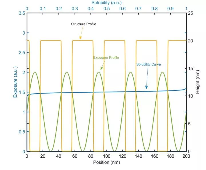
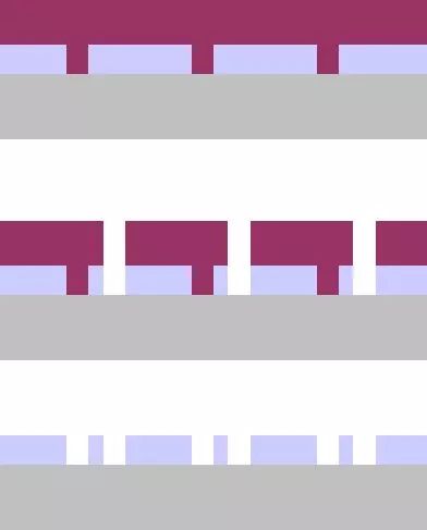
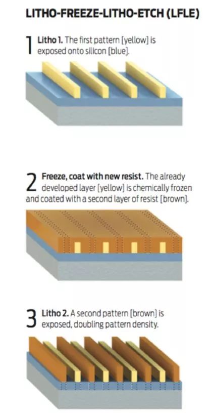
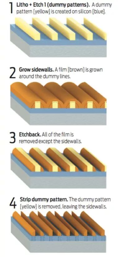
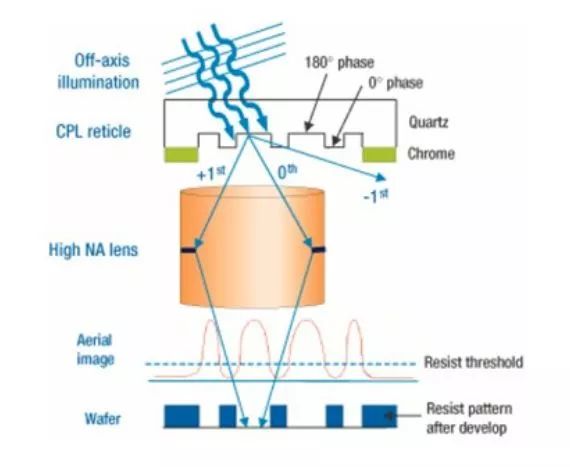
There is a problem in knowing, "How does a lithography machine in the chip industry sculpt a line width that is much smaller than its own wavelength?" This question is very interesting. With the change of semiconductor technology in one year, the materials that students see in school can't keep up. The EDN editor saw the reply of the netizen Ida Lin, and found it easy to understand. It was specifically authorized to share it with everyone. Of course, more professional explanations can also be found in the Wiki. Think of the entire chip industry, including Intel, GF, TSMC, Samsung all in the Samsung 22nm, 28nm this node for a long time, presumably encountered the limit of 193nm ArF. However, the 193nm can make the following 50nm, 1/4 wavelength scale, it is already amazing, isn't it? However, there are also naming issues behind this. The xx nm node does not mean that the real structure is as small. First of all, this number originally refers to the half pitch of the structure, which is half the period. By later, more water, generally refers to the smallest feature-size. For example, a row of 100 nm cycles of protrusions or depressions, the width of the protrusions is 20 nm, and the gap is 80 nm. This is not strictly a 20 nm process. In addition, 32nm 22nm 14nm is only a sign of a technology node, and the corresponding minimum structure may be 60nm, 40nm, 25nm, etc., in short, a lot more than the nominal. This node is not the same for each company, for example, people often say that Intel's 14nm is higher than Samsung's 10nm density and TSMC's (etc.). But how do you make a minimum-feature that is much less than half the cycle? From the light field distribution alone, the width of a peak or valley may not be able to break through the diffraction limit. But the nature of the photoresist can be exploited! The solubility of photoresist after exposure depends on the amount of exposure, which we all know, but the dependence is not linear. By controlling this non-linearity, the smaller ones will not be dissolved near a certain threshold exposure amount, and the larger ones are easily dissolved. By accurately grasping the exposure amount, the line width of the minimum structure can be easily controlled. Imagine a light field that is evenly distributed like a sine wave. Exposure will be controlled so that only those positions near the peak are completely dissolved. The solubility of other parts is not changed. Then the last structure to be made is the same as a sine wave with a period, but the minimum A much smaller structure. See below. The sag of the structure represented by the yellow curve is smaller than the width of one peak of the light field distribution. Of course, this method is not capable of making infinite features. After all, the solubility characteristics of photoresists are all there is to be what they want. The development of each formulation is very complex and must be matched with the existing process technology. In addition, the photoresist coating has a thickness, and the exposure distribution and the overall surface are not the same. At the same time, its mechanical properties can not maintain the narrow details of the integrity. There are other methods that can concentrate the area where the photoresist layer is activated to a much smaller scale than the exposure light field, including various chemical processes, heat treatments, and the like. Since the above method allows the Minimum Feature Size to be at least less than a half cycle, then it is possible to achieve a density increase - through multiple exposures. The same structure, doubled and doubled the density. However, implementation is not that simple. The key is to do a step in the subsequent exposure to freeze the previous structure protection. The most simple multi-exposure technique is to do it once and do it again, which can be called LELE (Litho-Etch-Litho_Etch). As shown below The top layer is a protective layer that has undergone a pattern (silicon color, such as SiN) plus a layer of photoresist (purple). The photoresist is carved into another set of grooves (center) under the new mask. The photoresist layer is finally removed, leaving a structure that can be further etched (below). Another variant is Litho-Freeze-Litho-Etch (LFLE). The second layer of photoresist is applied directly to the first layer of photoresist that has not been removed but is chemically frozen, and the lithography is again performed to form a double structure. More steps than LELE can save. The characteristic of this type of multiple exposure is that the process is simple and crude, and some people try to apply it very early. But one of the biggest problems is the problem of the latter lithography and the previous alignment. This is almost a huge obstacle that can completely invalidate such methods. To make a structure around 20nm, the alignment error should be controlled below 4-5nm. However, the SEM resolution that can be used to observe the best is 10nm! In short, this problem does hinder the application of this method - in addition to the early 45nm, 32nm node DRAM process (simple structure, high repeatability), and the situation of super light double exposure is almost no, CPU GPU chip should not be used much . Next is another smarter multiple exposure, which can be collectively referred to as SADP (Self-Aligning Double Patterning). For example, Side Wall Transfer is the core implementation. Mainly to use the Sidewall of the first layer structure to form twice the Feature, save a lot of things from the process, and do not have to consider the alignment problem. However, this method is also very technically demanding. Let me put another picture: Look at the deposition of brown material in the second step - this step is a Conformal Deposition - all surfaces have similar deposition rates regardless of orientation. The next step in the third step of etching should be a Non-conformal Etching—etching is performed almost vertically only to produce the desired effect. Both of these steps have limitations on materials and processes. One of the difficulties with Sidewall Transfer is that the Sidewall of the initial structure must be flat enough, otherwise the support of supplementary materials will be problematic, and the shape may deviate greatly, leading to deviations in the etching of the underlying material layers. And the degree of freedom is obviously higher in the former methods. The width, symmetry, etc. of the generated structure are all limited. However, this is not really a big problem. It can be considered when designing in the early stage. Mainly there is no alignment to this big problem, and the scope of application is much wider. Based on this method, SAQP can be achieved by repeating it once. It is not a problem to do a 20nm feature. There is also a wonderful way, Direct Self-Assembly - that is, using a layer of material for the Phase Seperation of the protective layer material can be used to do two non-influenced etching. Specifically, using a certain kind of copolymer, such as PMMA-PS, under the condition of satisfying certain molecular ratios and physical conditions, PMMA runs to the side and PS runs to the other side, forming a very orderly staggered structure and then performing different The etching of the components can be Double Pattern. However, there are many limitations to this method, such as the distribution of the staggered structure, the duty cycle, and not how you want people to be distributed. And the flatness is certainly inferior to those of Hard Mask Material. This method is currently still mainly used for academia to experiment with various small-scale simple structures and it seems to have not been applied to the industrial field. The above-mentioned various methods, combined with the actual point of view, due to the fact that the real integrated circuit structure is super complicated, various materials, different regions, different requirements for interconnection and disconnection, and the actual layout requires two-dimensional or even three-dimensional considerations All of these complex factors constitute more and more difficult problems, and shortcuts, from which derives the stunts based on different materials (dielectric layers, metals) and different functional areas. But this piece is too complicated and I don't know much about it. Say so much how to increase the density and reduce the line width through the means of lithography, but it also needs a core technology - how to make the most beautiful and the smallest single-exposure Feature/Period? Based on CD=k*lamda/NA, k is usually a constant between 0.25 and 1, so the first thing we would like to improve is NA=nsin (image square half aperture angle). The sine can be up to 1 and a layer of high-refractive liquid, such as water, is added between the objective lens and the wafer. The NA is 1.33. (should also be able to use higher refractive index oil to more than 1.4?). Immersion Lithography, not much to say, was a must-have before EUV (though it certainly won't work with EUV). Then Off-Axis Illumination. The main optical axis of the optical system and the illumination direction are different, and the light source is tilted. This principle is also more intuitive. It is to discard some of MASK's spatial low-frequency components as much as possible, and allow high-frequency components with finer structures to enter the objective lens for imaging. In principle, all high-frequency components smaller than the wavelength of light in the MASK become high-frequency information. The corresponding light is transmitted only in the transverse direction, and the axially very attenuated escaping wave may not be used. Objective lens collection. In the case of oblique illumination, at least one of the high-frequency spatial components has a smaller diffraction angle to enter the objective lens, and even changes from an evanescent wave to a component that can be collected (of course, the other one is pushed farther. But it does not matter). The final effect is that the image on the Wafer contains more high-frequency components and naturally comes closer to the Mask. Mask can also make a fuss. The first step is to use Phase-Shift Mask. The adjacent very wide apertures introduce different phase shifts. Then, in the case of coherent imaging, although the respective electric field intensity distributions of the two are greatly overlapped, after the electric field superposition, there is a (preferably pi) phase difference. It becomes one plus one minus, the center strength is zero, and it is divided into two separate peaks. The final key technology is Optical Proximity Correction. None of the above mentioned techniques can guarantee that the final structure will have a perfect, horizontal and vertical shape, and that the shape of a circle will be like a circle, especially for a 2D structure. Although a MOS tube does not need to have a perfect shape to guarantee the work, a large number of intensive work units and separate connections from each other must be guaranteed. To be sure, if you make MASK naive and look like the structure you want last time, then 100% of what you finally get at 65nm is a stack of rubbish. OPC magic figure: How is this process achieved? I do not know, but it is necessary to use very complex wave optic simulation methods and countless experimental feedback and subsequent optimization. From some perspectives, the OPC area seems to be the most popular work on the front line of FAB (it is purely hearsay and accuracy is not guaranteed). Finally, I am not a practitioner. I am purely for the presentation of the course. I am interested in this matter and collected a series of materials. My confusion has always been to discover that these materials are very fragmented and trivial. I rarely see large-scale articles or magazine topics. I don't know whether they are due to trade secrets or anything, but I can feel that they are not in the academic world. After all, everyone is playing Graphene, CNT, TMD, Single-Molecule Transistor is not it? silicon? This stuff should be 30 years old. I personally have many problems that I have not been able to solve for years. For example, from which node did Multi Patterning begin to be widely adopted? 65?45? EUV has talked for so many years, is it shaping now, what technology is the mainstream of 14nm and 10nm? After all, such a huge investment and technology conversion, there is no possibility of D/E mixing it? In fact, it is quite magical to think about it. In the past five years, due to the technical bottleneck, the semiconductor technology industry did not know that there were several rounds of tremendous technological innovations and changes. However, the outside world couldn’t see any major movements. Basically, each year can be a simple one. child. The stability of this kind of output is really a bit meticulous. About the Sidewall section, Zhihu User Albert Hu made his own answer: Why 193nm wavelength light can be used in the 130nm, 90nm, 65nm or even 45nm process? Because the polysilicon strip below 130nm gate generally uses Sidewall Transfer, not directly using lithography. In simple terms, the side wall The transfer is first patterned by photolithography or the like. The pattern does not need to be very fine, but after some processing, the edges are made to be stair-like and relatively steep. A layer of the desired material is then deposited so that the edge of the pattern will also have a layer of material of controlled thickness forming the same step. The extra material on the upper and lower planes is etched away, leaving a very thin one at the step. The width of this material depends on the choice of materials and the way and duration of deposition, so photolithography wavelength does not work. Its accuracy depends on the "material wavelength" of the material (and the etched material). The real use of photolithography is in the interconnect layer, and the minimum spacing of the lowest level interconnect layer under the 65nm process is currently also above 120nm and has not yet reached the Rayleigh limit of 193nm lithography. Using this scheme, the 193nm wavelength is Can be used on the 90nm, 65nm or even 45nm process. More specifically, the line width has lost contact with photolithography wavelengths. Half-generation and even more exotic line widths can be achieved on the same device. The 80nm production equipment may be the same as 90nm, 55nm and Like 65nm. The gap between the half generations and even the two generations has become very small. The line width almost becomes the least important parameter in the process. Pmic Hot Swap Controllers,Pmic Hot Swap Controllers Ec-Mart,Management Pmic Hot Swap Controllers,Hot Swap Voltage Controllers Shenzhen Kaixuanye Technology Co., Ltd. , https://www.iconlinekxys.com