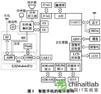
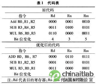
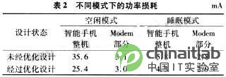
introduction This article refers to the address: http:// With the continuous development of the communication industry, mobile terminals have evolved from a single call function to voice, data, image, music and multimedia. For mobile terminals, there are basically two types: one is a feature phone; the other is a smart phone. Smartphones have the basic functions of traditional mobile phones and have the following features: open operating system, hardware and software scalability and support for secondary development by third parties. Compared with traditional mobile phones, smart phones are increasingly favored by people because of their powerful functions and convenient operation, and will gradually become a trend in the market. However, as a portable and mobile terminal, it relies entirely on the battery to supply power. As the function of the smart phone becomes more and more powerful, its power loss is also increasing. Therefore, it is necessary to increase the usage time and standby time of the smartphone. There are two solutions to this problem: one is to use a larger capacity mobile phone battery; the other is to improve the system design, using advanced technology to reduce the power loss of the mobile phone. At this stage, the battery equipped with mobile phones is mainly lithium-ion batteries. Although the energy density of lithium-ion batteries has increased by nearly 30% compared with the past, it still cannot meet the development needs of smartphones. As far as the lithium ion battery materials currently in use are concerned, the energy density is only about 20% of the lifting space. Another fuel cell that is widely regarded as the future development trend of mobile phone batteries in the industry can make the talk time of smartphones exceed 13 hours and the standby time is up to 1 month. However, this battery technology is still immature, and it is still commercial. For a while [1]. Increasing the overall trend of mobile phone battery capacity will increase the cost of the whole machine. Therefore, starting from the overall design of the smartphone, advanced technology and devices are applied to design a solution that reduces power loss, thereby maximizing the use time and standby time of the smartphone. In fact, low-power design has become an increasingly pressing issue in smartphone design. 1 Smartphone hardware system architecture The hardware architecture of the smartphone discussed in this article uses a dual CPU architecture, as shown in Figure 1. The main processor runs an open operating system and is responsible for the control of the entire system. The DBB (Digital Baseband Chip) from the processor is a wireless Modem part, which mainly performs A/D conversion, D/A conversion of the voice signal, codec of the digital voice signal, channel codec and timing control of the wireless Modem part. The master and slave processors communicate through the serial port. The main processor uses XXX's CPU chip, which adopts CMOS technology, has ARM926EJ-S core, adopts ARM's AMBA (advanced microcontroller bus architecture), contains 16 kB instruction cache and 16 kB data cache. And MMU (memory management unit). In order to implement real-time video conferencing, an optimized MPEG4 hardware codec is carried. It can perform hardware processing on large-quantity MPEG4 codec and voice compression decompression, which can alleviate the computational pressure of the arm core. The main processor includes an LCD (Liquid Crystal Display) controller, a camera controller, SDRAM and SROM controllers, many general-purpose GPIO ports, and an SD card interface. These make it an excellent application in the design of smartphones. In the hardware architecture of the smart phone, the wireless modem part only needs to add certain peripheral circuits, such as audio chip, LCD, camera controller, microphone, speaker, power amplifier, antenna, etc., which is a complete ordinary mobile phone (traditional mobile phone). Hardware circuit. The analog baseband (ABB) voice signal pin communicates with the audio codec chip to form a voice channel during the call. From the system architecture of this hardware circuit, the most power-consuming part includes the main processor, wireless modem, LCD and keyboard backlight, audio codec and power amplifier. Therefore, how to reduce their power consumption in design is an important issue. 2 low power design 2.1 Reduce the supply voltage and frequency of the CPU part In digital integrated circuit design, the static power consumption of CMOS circuits is very low, which is basically negligible compared with its dynamic power consumption, so it is not considered. Its dynamic power calculation formula is: Pd=CTV2f (1) Where: Pd is the dynamic power consumption of the CMOS chip; CT is the load capacitance of the CMOS chip; V is the operating voltage of the CMOS chip; f is the operating frequency of the CMOS chip. It can be known from equation (1) that the power consumption in the CMOS circuit is linear with the switching frequency of the circuit, and has a quadratic relationship with the supply voltage. For the CPU, the higher the Vcore voltage, the faster the clock frequency, the greater the power consumption. Therefore, under the premise of being able to normally satisfy the system performance, the CPU with low voltage operation should be selected as much as possible. For the CPU that has been selected, reducing the supply voltage and operating frequency can achieve better results in overall power consumption. For the main CPU, the core supply voltage is 1.3 V, which is already very small, and the main frequency of the full-speed operation can be set as needed. The other various frequencies required internally are generated by the main frequency division. The main CPU frequency fCPU calculation formula is as follows: On the COMS chip, in order to prevent damage caused by static electricity, unused pins cannot be left floating. Generally, pull-down resistors are used to reduce the input impedance and provide a discharge path. A pull-up resistor is needed to increase the output level, thereby increasing the noise margin of the chip input signal to enhance the anti-jamming capability. However, when selecting a pull-up resistor, the following points must be considered: a) Considering the power consumption and the chip's current sinking capacity, the pull-up resistor should be large enough to reduce the current; b) From the perspective of ensuring sufficient drive current, the pull-up resistor should be small enough to increase the current; c) In high-speed circuits, excessive pull-up resistors can flatten the edges of the signal and deteriorate signal integrity. Therefore, in consideration of the ability to drive the latter stage normally (ie, considering the VIH or VIL of the chip), a larger resistance value is selected as much as possible to save power consumption of the system. For pull-down resistors, the situation is similar. 2.3.2 Processing of Floating Pins For the floating pins of CMOS devices in the system, attention must be paid. Because the input impedance of the CMOS floating input is extremely high, it is likely that some charge is induced to cause the device to be broken down by high voltage, and the signal level of the input terminal is randomly changed, causing the CPU to be constantly woken up during sleep, so that it cannot enter the sleep state. Or other inexplicable failures. So the correct way is to keep the unused input connected to the corresponding supply voltage to maintain a high level or to keep it low by grounding, depending on the initial state of the pin. 2.3.3 Buffer selection Buffers have many functions, such as level shifting, increased drive capability, direction control of data transmission, etc. When adding buffers based solely on drive capability considerations, care must be taken that more energy is wasted due to excessive drive currents. Drop it. Therefore, it should be carefully checked whether the maximum output current IOH and IOL of the chip are enough to drive the lower level chip. When selecting the appropriate front and rear stage chips, the buffer should be avoided as much as possible. 2.4 power supply circuit Due to the dual CPU architecture, there are many peripherals and many different power supplies are required. In the case of the main CPU alone, 1.3V, 2.4V, and 2.8V are required, so many voltage change units are required. Generally, there are several voltage conversion methods: linear regulator; DC/DC; LDO (low drop regulator). Among them, LDO is essentially a linear regulator, mainly used in the case of small voltage difference, so it is combined into a linear regulator. Linear regulators are characterized by simple circuit structure, low component count, and large input and output voltage differences, but their Achilles heel is low efficiency and high power consumption. The efficiency η depends entirely on the output voltage. The DC/DC circuit is characterized by high efficiency and flexible lifting and lowering voltage. The disadvantage is that the circuit is relatively complicated, the ripple noise is relatively large, the volume is relatively large, and the price is higher than the linear voltage regulation. For boosting, only DC can be used. /DC. Therefore, in the design, the power supply ripple noise is not strict, the use of DC / DC voltage conversion device, which can effectively save energy and reduce the power consumption of smart phones. 2.5 LED light control In smartphone circuits, keyboards and LCD backlights consume a lot of energy when working. For example, the LCD used in the architecture of this paper has the following electrical requirements: the forward current is typically 15 mA, the forward voltage is typically 14.4 V, and the backlight power consumption is typically 216 mW. It can be seen that the LCD background LED lamp consumes a lot of power during normal operation. Therefore, in the design, the power consumption of the LED lamp must be reduced. You can do the following: a) Short-circuit a small resistor in the LED lamp circuit to change the resistance value to control the current when the LED lamp is working. b) Using the hysteresis effect of the human eye, a PWM (Pulse Width Modulation) signal is used to control the switching of the LED lamp. In the main CPU, GPIO20-GPIO23 and GPIO2-GPlO5 can be configured as PWM signal output through configuration registers GPCON_U and GPCON_L, and then the corresponding internal registers can be configured to control the frequency and duty cycle of the PWM output signal as control pins. LED backlights to reduce the power consumption of LCD backlights. c) Provide an interface for adjusting the brightness of the backlight on the graphic interface of the mobile phone, so that the user can further adjust the brightness of the backlight of the backlight based on the brightness of the LED light set by the system, thereby increasing the flexibility of the use of the mobile phone and further reducing The power consumption of the phone. 2.6 Control of the wireless Modem part As shown in Figure 1, the hardware architecture of the smartphone adopts a dual CPU architecture. The wireless modem is used as a peripheral of the main CPU, which has its particularity compared with other peripherals of the main CPU chip, for example, when the smartphone is in sleep mode. When you can directly turn off the power supply of peripherals such as LCD and camera, and the wireless Modem does not work, you must require the wireless modem to continue to wait for incoming calls, search the network, etc., but not directly shut it down. For the wireless Modem solution in the hardware architecture of this paper, there is also a system that runs a complete GSM (Global System for Mobile Communications) protocol and an independent power management module. The main CPU can negotiate power management through the UART port and the wireless Modem. The power management inside the wireless Modem is controlled by itself. When the wireless Modem is in the idle state, it can enter and exit the standby mode intact. Therefore, in the design of the hardware architecture of this article, when the smart phone is powered on, when the wireless modem is powered on and off, the Modem is powered off. 2.7 Software Optimization Where: m=MDIV+8; p=PDIV+2, s=SDIV; MDIV, PDIV and SDIV can be set by register. Therefore, the design determines the main CPU frequency is a key to the overall system power and performance. Based on the comprehensive consideration of system performance and power consumption, this paper sets the main CPU frequency to 204 MHz. 2.2 DPM DPM (Dynamic Power Management) is to save power by dynamically controlling the clock or voltage of the system during system operation. This dynamic control is closely related to the operating state of the system. This work is often implemented by software [3, 4]. 2.2.1 Defining different working modes In the hardware architecture, the working mode of the smartphone is closely related to the working mode of the main CPU. In order to reduce power consumption, the main CPU defines four working modes: General Clock Gating mode; IDLE mode: SLEEP mode; Stop mode. In the case that the main CPU frequency is determined, the corresponding four working modes are defined in the smartphone: normal working mode (Normal); idle mode (Idle); sleep mode (Sleep); and off mode (OFF). The various modes are described as follows: a) Normal working mode: The main CPU works in the General Clock Gating mode; the main CPU runs at full speed; the clock frequency is 204 MHz. In this state, the smartphone consumes the most power. According to different operating states, such as playing MP3, making a call, and actually measuring, the working current of the smartphone in this mode is about 200 mA. b) Idle mode: The main CPU operating mode is Idle mode, the main CPU main clock is stopped; the clock frequency is 204 MHz. In the idle state, the keyboard backlight and LCD backlight are turned off, and there is a standby screen on the LCD. The specific event can make the smartphone idle mode enter the normal working mode, such as clicking the touch screen, timing wake-up, button, incoming call, and the like. c) Sleeping eye mode: The main CPU working mode is SLEEP mode, except that the wake-up logic inside the main CPU is turned on, and the rest is fully turned off; the main CPU clock is a slow clock using 36.768 kHz. Except for Modem, all peripherals are turned off, and the short-time pressing of the power-on button is made to wake up the smartphone from sleep mode to normal operation. d) Shutdown mode: The main CPU works in stop mode, except for the main CPU leakage current, which does not consume power; the main CPU is turned off. The smartphone must be turned back on before it can enter the normal working mode. Actually, the current of the mobile phone in this mode is 100μA. From the above, the power of the smartphone in the normal working mode is much larger than in the idle mode and the sleep mode. Therefore, when the user does not operate the mobile phone, the software is set to enable the mobile phone to enter the idle mode or the sleep mode as soon as possible; when the user operates the mobile phone, the main CPU is woken up by the corresponding interrupt, so that the mobile phone returns to the normal working mode, and the processing is finished. The responsive event quickly enters idle mode or sleep mode. 2.2.2 Turn off idle peripheral controllers and peripherals In the architecture of the hardware system, it can be seen that the main CPU is externally connected with many external devices such as LCD, camera, IrDA (infrared adapter), Bluetooth, audio codec, power amplifier and the like. When the smartphone is in the normal working mode, the peripheral device in the idle state can control the LDO or DC/DC power chip that supplies power to the peripheral device through the GPIO port of the main CPU, and close the power supply chip of the peripheral device to achieve Turn off the purpose of the peripheral. Especially for high-power peripherals, they must be reliably turned off. For some working peripherals, such as audio codecs, by setting internal registers, turn off channels, power amplifiers, D/A converters, etc. that are not used inside the chip to reduce the power consumption of these devices. For the various Interface Controllers of the main CPU, it is generally not used. Even if the smart phone is in the normal working mode, the usage status of various interface controllers is different in different operating states; the interface controller is not in the working state. If you do not turn it off, it will still consume current. For the main CPU, the current consumption of each peripheral interface controller [2] is as follows: NAND Flash is 2.9 mA; LCD is 5.8 mA; USB HOST is 0.4 mA; USB driver is 2.9 mA; timer is 0.5 mA; SDI It is 1.9 mA; UART is 3.6 mA; RTC is 0.4 mA; A/D converter is 0.4 mA; IIC is 0.6 mA; IIS is 0.5 mA; SPI is 0.5 mA. In the smartphone hardware architecture shown in Figure 1, the SPI interface and USB HOST interface are not used, so the SPI and USB HOST interfaces can be permanently turned off by setting the SPCONO and HcControl registers, which saves 0.9 (0.5 + 0.4) mA. . When the smartphone is in normal working condition, the idle interface controller can be turned off to further reduce the power consumption of the smart phone, and also prevent the influence of the reverse current on the bus. 2.3 Low-power design of interface driver circuit When selecting a peripheral chip of a smartphone such as an SDRAM, an LCD, a video camera, an audio codec, etc., in addition to considering its performance, it must also consider the power consumption during normal operation. There are several factors that must be considered when designing an interface circuit: 2.3.1 Selection of Pull-up/Pull-Down Resistors Software optimization is an important task that can greatly improve the efficiency of software running and reduce the power consumption of software running. For example, the reordering of instructions can eliminate the failure of the instruction pipeline caused by load delay, branch delay, jump delay, etc. without affecting the execution result of the instruction [5]. As shown in the arm assembly shown in Table 1, after converting the instructions into binary encoding, the difference is that the binary encoding of each register operand is different. According to Table 1, from the electrical performance point of view, by reducing the Hamming distance between successive instructions, the original code is changed six times more than the optimized code bit, and the two sets of codes achieve the same function, therefore, The power consumption of the optimized instruction execution is smaller than the original instruction. Therefore, after the system software is completed, the software can be reduced in power consumption by optimizing the code while ensuring that the software functions are consistent. 3 test results and discussion In the design of the smartphone, the power loss of the smartphone in idle mode and sleep mode is measured by continuous hardware optimization and dynamic management of the power in the software. The results are shown in Table 2. As can be seen from Table 2, after optimization, the current value of the smartphone is reduced by 10.2 mA in idle mode and 1.5 mA in sleep mode. For the wireless Modem, because it has an independent power management module, it is basically at around 3 mA, with little change. Compared with the unoptimized design, the smart phone has been optimized to reduce power consumption in sleep mode and idle mode. Under the same battery capacity, the standby time and usage time of the smartphone are greatly improved. Therefore, by the above method, the power consumption of the smartphone can be effectively reduced. With the development of mobile phone technology, especially in the design of smart phones, low-power design will become an increasingly urgent problem. With the advent of some new technologies and their application in smartphone design, such as advanced power management chips and advanced processors, designers are provided with greater flexibility to significantly reduce smartphone power consumption. However, as a designer, in system design and software programming, it is necessary to consider how to reduce the power consumption of the system from time to time. Only in this way can the designed system have a good performance and be favored by users. Interface Controllers Interface Controllers,Asus Control Interface,Enhanced Host Controller Interface,Dc Motor Interface With Arduino Shenzhen Kaixuanye Technology Co., Ltd. , https://www.icoilne.com