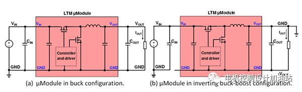
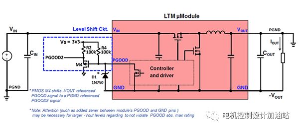
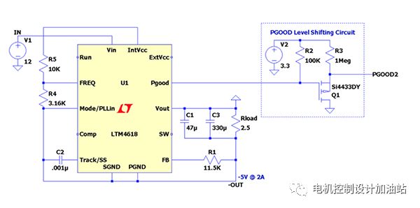
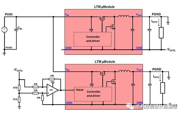
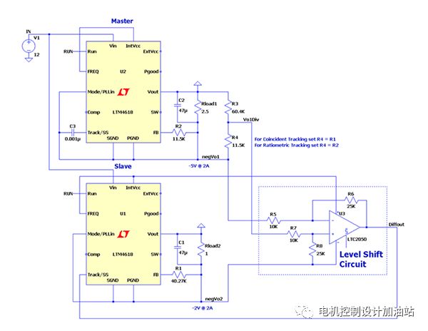
Linear μModule regulators are ideal for point-of-load power supplies because they are easy to plug in, compact, and integrated design. They can be adapted to tight spaces with very little engineering work-only a few components are required in addition to the μModule package itself. Any step-down μModule regulator can be used to effortlessly generate a negative voltage solution while retaining the conventional simple design and low component count inherent in the μModule regulator. Three steps for negative voltage output The following three simple design steps convert the buck topology to an inverting buck-boost topology, producing a negative output voltage rail. Connect the V OUT pin of the μModule regulator to the system ground (PGND). This creates the ground inductance configuration required for the inverting buck-boost converter. Supply power to the converter by connecting the input power between the V IN pin of the μModule regulator and PGND. The GND pin of the μModule regulator is now the negative output voltage rail (-V OUT). The load is connected between the negative output and PGND. As shown in the standard step-down configuration of Figure 1(a), using a μModule regulator (such as LTM4601) requires a small amount of input and output capacitors to generate a fully functional step-down DC/DC converter. In this configuration, the output pads of the μModule regulator are connected to their corresponding voltages, that is, the V OUT pad is connected to the external V OUT and the GND pad is connected to the external GND. If the external connection is changed to the configuration shown in Figure 1(b), the step-down μModule regulator will become an inverting buck-boost converter. Here, the V OUT pad of the μModule regulator is connected to the external GND, and the GND pad becomes negative V OUT. Therefore, the μModule regulator GND refers to -VOUT. Figure 1. Only a few connection changes convert a step-down μModule regulator (a) to a negative output regulator (b) Level shift control signal Due to the difference in ground level (PGND and GND), configuring the control circuit requires more consideration than the power level. The μModule regulator refers to the pin voltage of its own GND pin, but the output voltage it provides is relative to the system ground (PGND). In this configuration, to transmit any PGND-referenced external control signals (such as RUN, TRACK, PGOOD, etc.) to the μModule regulator, the signal needs to be converted to the ground reference GND (-V OUT) of the μModule regulator. Figure 2. The input signal of the μModule regulator must be converted from the power ground level to the -VOUT reference level The following circuit example shows how to level-shift the system ground reference signal for RUN, PGOOD and TRACK pin compatibility. Run level conversion By applying an enable signal to the pin, the RUN pin input allows the μModule regulator to be turned on and off. In many cases, the module can be enabled by the pull-up resistor between V IN and RUN pin and V IN, but if the RUN pin is to be controlled by an external PGND reference signal, additional considerations are required. Imagine what would happen if we applied the PGND reference enable signal (V EN) directly to the RUN pin of the negative converter without using a level conversion circuit. Since the voltage seen by the μModule regulator on its RUN pin is V EN + | -V OUT |, (depending on the set output voltage), we may exceed the absolute value of the pin. maximum. Rated voltage (and cause damage to parts). In addition, once the μModule regulator is turned on, the enable signal may not be enough to turn off the μModule regulator. Therefore, we need a circuit to convert the PGND reference enable signal to a level suitable for the RUN pin of the μModule regulator. The simple circuit in Figure 3 uses an enable signal based on PGND, and the level reduces it to a voltage level suitable for the RUN pin. In the circuit where the enable signal is high, the PNP transistor Q1 is turned on to generate a bias current with Rb and Rc to make the RUN pin voltage higher than its threshold and turn on the μModule regulator. The maximum voltage of the D1 pin is clamped to prevent exceeding the absolute value of the pin. Maximum rating. When the enable signal is low, Q1 is turned off and resistor R3 discharges the RUN pin to below the threshold to turn off the μModule regulator. Note that the μModule regulator package may already contain resistor R3 and/or Zener diode D1. Please refer to the data sheet for details. Figure 3. Level shift enable circuit Figure 4 shows the setting of the RUN pin level shift circuit used in the negative output configuration of the LTM4609. V IN = 10V, -V OUT = -12V @ 2A. Figure 4. LTM4609 with level translation enable circuit PGOOD level conversion The PGOOD output pin indicates whether the output voltage of the μModule regulator is within the regulated (PGOOD high level) range (PGOOD low level). The PGOOD pin inside the module is an open-drain MOSFET, so a pull-up resistor is needed to provide the bias voltage. If you want to use the PGOOD function in a negative output configuration, the PGOOD signal seen by the μModule regulator must be appropriately level-shifted to the PGND reference signal for further use by the system. Imagine what happens if we directly use the PGOOD output signal of the module without any level conversion circuit. Since the PGND on the PGOOD pin is referenced to the pull-up power supply (VS), because the maximum voltage of the module on its PGOOD pin is VS + | -V OUT |, the absolute voltage of the pin (depending on the set output voltage). The maximum rating can be exceeded. Also in this setting, when the module PGOOD pin signal is low, the PGOOD signal relative to PGND may not be suitable for use in the system (that is, PGOOD low signal level The simple circuit in Figure 5 uses the GND pin of the μModule regulator as the PGOOD signal and converts its level to the PGND reference signal PGOOD2, which is suitable for further use of the system. In the circuit, when the module outputs a PGOOD high level signal, PMOS M4 turns off, and R2 pulls PGOOD2 high to provide the voltage Vs. Zener diode D1 protects the PGOOD pin from exceeding its absolute value. maximum. score. When the module outputs a low level signal of PGOOD, M4 opens and pulls PGOOD2 down to system ground. Please note that if VS + | -V OUT | Zener diode D1 can be omitted Figure 5. PGOOD level conversion circuit The following examples illustrate the setting of the PGOOD pin level conversion circuit when using the LTM4618 in the negative output configuration. V IN = 12V, -V OUT = -5V @ 3A. Figure 6. LTM4618 with PGOOD level conversion circuit Tracking level shift The TRACK pin input allows the μModule regulator to track the output voltage of another power rail by providing a tracking signal (ie, a divided version of the output voltage rail of the main μModule regulator) to the TRACK pin of the slave μModule regulator Slope. The TRACK pin voltage seen by the internal controller of each μModule regulator is related to its μModuleGND pin, but in applications that need to configure two negative output converters for tracking, the GND pin of the μModule regulator can be at a different The potential. The potential difference between the master and slave GND pins means that the tracking signal provided by the master device cannot be directly applied to the tracking pins of the slave device. In these types of applications, additional considerations are required to ensure that the slave phase can see the correct reference tracking signal from the master phase. In the simple circuit in Figure 7, the GND pin of the main microcontroller refers to the tracking signal (Vo1Div-negVo1) provided to the input of the differential amplifier. The differential amplifier is powered by a power supply that is referred to the GND pin of the μModule regulator of the slave module (in this case, it is powered by the INTVCC regulator of the slave module). Since the amplifier is based on the GND pin of the μModule regulator of the slave module, its output signal is a level-shifted version of the input tracking signal, which is correctly referred to the GND pin of the slave device. Then the output signal of the amplifier is applied to the TRACK pin of the slave, allowing the slave to track the movement of the output rail voltage of the master. Figure 7. Track level shift enable circuit Figure 8 shows the tracking performance of two LTM4618μModule regulators configured in a negative output configuration using the tracking pin level shift circuit. V IN = 12V, -V OUT1 = -5V @ 2A, -V OUT2 = -2V2A. Figure 8. LTM4618 tracking of negative V OUT in conclusion The μModule regulator enables designers to produce negative output applications as effortlessly as positive products. In fact, any standard step-down μModule regulator demo board can be easily configured for negative output applications. This article summarizes the control circuit design considerations caused by the relative ground level difference between the power ground and μModuleGND (-V OUT). Mini Sas Sff-8088,Mini Sas 26P Sff-8088 Cable,Mini Sas 26P To 4Sata Cable,Sff-8087 To Mini Sas 36P Dongguan Aiqun Industrial Co.,Ltd , https://www.gdoikwan.com