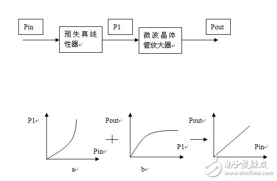
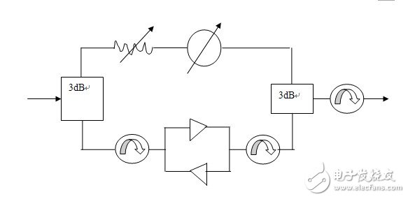
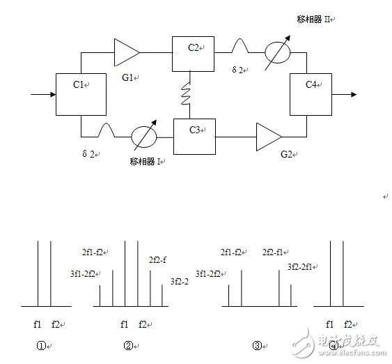
The nonlinear problem of microwave power amplifiers is a problem worthy of attention in many fields of application. For example, power amplifiers in satellite transponders of satellite communication frequency division multiple access (FDMA) systems generally have to amplify multiple addresses. The carrier (several, dozen or even hundreds of carriers) is in multiple carrier operating states. If the power amplifier is operating near saturation at this time, it will cause distortion due to the nonlinearity of the amplifier. Therefore, the linearization of the amplifier has caused great concern. In the low frequency band, the most common way to improve the linearity of the amplifier is to use negative feedback technology. In the low frequency band, the phase shift of the signal due to its inherent delay is small. This phase shift is negative feedback. The effects of the amplifier are not apparent over a wide frequency band. In the microwave band, the delay effect of the amplifier is already obvious. If negative feedback is used to improve the linearity of the amplifier, the amplifier can only work stably in a very narrow frequency band. Therefore, in order to improve the linearity of the microwave transistor amplifier, other measures must be taken. One of the more frequently used linearization measures is the back---off technique. The so-called compensation is to reduce the input power, so that the working point of the amplifier is farther from the saturation point, and it works in the range of the OA segment as shown in the figure. The linearity of the pout---pin curve of a segment shows that compensation is to reduce the nonlinear distortion by reducing the output power. This method is simple, and the amplifier can obtain higher linearity. However, since the DC operating state of the transistor amplifier is unchanged, the power of the amplifier is correspondingly reduced, and the transistor itself is also "overkill", and its capability is not fully exerted when needed. For large power output, it is necessary to use a transistor that can output more power, and the device also puts forward higher requirements. These shortcomings of compensation technology limit its wide range of effects. Figure 1. Transistor amplification curve In order to obtain both large output power and high linearity, in the microwave transistor power amplifier, in addition to selecting a transistor with good performance and reasonably selecting the working state of the transistor, effective linearization must be adopted. Measures. At present, the linearization measures that are attracting attention include PredistorTIon technology and feed-for-word technology. These two technologies are introduced below. The predistortion technique involves inserting a linearizer in front of the microwave transistor amplifier to compensate for the distortion of the amplifier with the distortion characteristics of the linearizer. Figure 2 is a block diagram of the predistortion technique and a schematic explanation of the nonlinearity of the compensation amplifier. Figure 2a is a schematic diagram of the input and output curves of the predistortion linearizer. Figure 2b is a schematic diagram of the input and output curves of the microwave transistor amplifier. It can be seen that the output signal of the predistortion linearizer enters the amplifier for amplification, thereby compensating for the nonlinear characteristics of the amplifier and improving the linearity of the amplifier. The structure of the predistortion linearizer has a variety of structures. Figure 3 is one of them. The input signal is first divided into two signals with a phase difference of 90 degrees through a 3dB coupler, one through a linear branch with an adjustable phase attenuator, and the other. All the way through a "non-linear branch" consisting of two anti-parallel microwave diodes, and then combined by a 3dB coupler to synthesize the output. Figure 2, predistortion technology circuit combination and principle description The signal through the "linear branch" increases linearly with the increase of the input signal, and the increase of the signal through the "non-linear branch" does not exhibit linearity. According to the nonlinear characteristics of the microwave diode, the input signal is small, the diode attenuation is large, and the input is small. When the signal is increased, the diode is small, so that the two signals with a phase difference of 90 degrees can obtain the curve characteristics in the figure when the input 3dB coupler is synthesized. Figure 3. A predistortion linearizer circuit Figure 4. Schematic diagram of feedforward circuit and spectrogram of each point The basic working principle of the feedforward circuit can be illustrated by the circuit combination block diagram and the spectrum diagram in FIG. The feedforward circuit consists of four directional couplers (C1, C2, C3, C4), two phase shifters (δ1+ fine-tuning phase shifter I, δ2+ fine-tuning phase shifter II), an adjustable attenuator, and a main amplifier G1. , an auxiliary amplifier G2. Among them, G1 is an amplifier that needs to improve linearity. The input is a signal with a frequency of F1+F2, and its spectrogram is 1. It is divided into upper and lower branches by a directional coupler. The upper branch signal is amplified by the amplifier G1. Due to the nonlinearity of the amplifier, the output produces a new frequency component. For example, the third-order and fifth-order intermodulation components have a spectrogram of 2, and the output is divided into two by the directional coupler C2, one phase is shifted by the phase-shifted δ2+ fine-tuning phase shifter II into the directional coupler C4, and the other path is entered through the attenuator. Directional coupler C3. Since these two paths are linear branches, the signal spectrum of the directional coupler C3 and C4 is 2, the input end is directional coupler C1, and the signal entering the lower branch is then phase-shifted by the phase shifter δ1+ fine-tuning phase shifter I Entering the directional coupler C3, since the branch is a linear branch, its spectrogram is still 1, adjusting the attenuator and fine-tuning the phase shifter I, so that the F1 and F2 frequencies in the two signal spectra entering the directional coupler C3 The signals cancel each other out. The spectrum of the C3 output signal is 3, which has only the third-order and fifth-order intermodulation components. The signal enters the amplifier G2. Since G2 only amplifies the small signal, it is considered to be in linear amplification, so the spectrum of the G2 output signal. 3, adjust the G2 gain and fine-tune the phase shifter II, so that the third-order and fifth-order intermodulation components entering the directional coupler C4 are offset one by one. As a result, the output of G4 has only F1 and F2 frequency components, and the spectrum of the spectrum is 4 . Comparing the input and output spectrums 1 and 4, it can be seen that the linearity of the entire amplifier is greatly improved. The variable attenuator can be electrically controlled by a PIN tube, and the circuit of the PIN tube can be controlled to continuously change the attenuator in the range of 0-20 dB. The trimmer phase shifter is an analog phase shifter consisting of a varactor diode and a 3dB bridge. The bias voltage on the varactor diode is continuously changed to change the phase of the output phase of the phase shifter relative to the phase of the input signal. degree. In order to ensure the communication transmitter output power is suitable, the frequency meets the requirements and the stable radio frequency communication signal, the more complicated signal detection and control circuit is usually adopted in the RF power amplifier circuit, and they cooperate with each other under the unified coordination of the microcontroller. Since the RF power amplifier has a high operating frequency, high power, and components operating at the extreme edge, it is important to monitor and protect it. Modern communication devices widely use microcontrollers in RF power amplifier circuits to detect, adjust, and control the operating state of the circuit. Figure 5 is a block diagram of the microcontroller control power amplifier circuit. It mainly completes power level control, automatic level control, antenna open circuit protection, load mismatch protection, temperature detection, receive/transmit conversion, input and output power indication, power supply voltage undervoltage indication, fault indication and alarm. Through the positive and negative power detection, current detection, load static detection and temperature detection, the working state information of the power amplifier circuit is sent to the microcontroller through the forward channel, and the micro-controller analyzes and processes the corresponding circuit in the power amplifier through the backward channel. Control adjustment ensures that the power amplifier always works in good working condition. Gel Battery,Gel Cell Battery,Gel Battery For Car,Gel Type Battery Power X (Qingdao) Energy Technology Co., Ltd. , https://www.solarpowerxx.com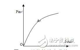
Research on Key Technology of Microwave Linear Power Amplifier