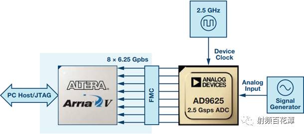
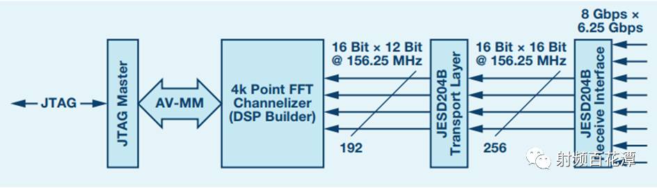
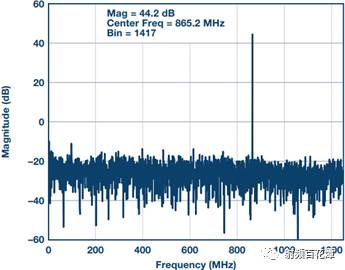
Modern electronic warfare (EW) system developers face numerous challenges, including increasing spectrum congestion and monitoring for wider bandwidth with higher detection sensitivity. In addition, system developers are under tremendous pressure to reduce development time, and many existing development models are difficult to cope with, requiring a variety of custom hardware and firmware designs to increase performance levels under the triple limits of size, weight and power. The new Gigabit-Sampling (GSPS) high-speed converters, high-performance FPGAs, and FPGAIP cores are beginning to change the landscape, bringing designers off-the-shelf solutions and configurable building blocks to help them face the next generation of challenges. A reference design using an ADI GSPS ADC with Altera® FPGAs and channelized IP will show us how designers can create state-of-the-art electronic intelligence and digital RF memory system solutions with reduced time-to-market. Electronic warfare systems can identify and counter electronic threats such as surveillance and tracking radars. Electronic warfare systems are generally classified into three categories: electronic support (ES), electronic attack (EA), and electronic protection (EP). Electronic support systems are used to intercept and measure signal parameters to identify signal sources and perform threat analysis. Electronic attack systems generate interfering signals to suppress real pulses. Digital Radio Frequency Memory (DRFM) is a spoofing technique used to deceive radar. Electronic protection systems are primarily used to process and store input signals to build a signal database. The database is a continuously updated lookup table for identifying future radar systems. Traditionally, these systems were developed on an analog platform. Modern systems are more digital and can take advantage of the powerful signal processing capabilities of programmable logic devices. In these systems, the detection of unknown target threats requires a receiver that can operate in a wider frequency band to identify threats and launch countermeasures. Typical electronic warfare systems operate from DC to 20 GHz. In addition to the wide bandwidth requirements, the actual electronic warfare system also requires high dynamic range, high sensitivity and accurate pulse characterization performance, and the new system also monitors the target bandwidth with faster speed and higher sensitivity. The input signals received by the electronic warfare system may come from many different sources and need to identify and distinguish each source, at which point the situation becomes more complicated. In addition to the intentional interference of the enemy, the increasing spectrum congestion, especially the spectrum congestion caused by the rapid expansion of the communication infrastructure, further increases the difficulty of effective detection. Complex systems that are smaller, lighter, and less powerful make the development cycle longer. However, a new generation of off-the-shelf solutions and programmable building blocks provide solutions to these challenges. For any EW system, the two key building blocks are analog-to-digital converters and real-time channelized IP, and we'll take a closer look at these two key building blocks to show how these challenges can be addressed. In many cases, the transition of high-speed ADCs from the analog domain to the digital domain is a limiting factor for electronic support systems, electronic attack systems, and electronic protection systems, where system architects often face a challenge. Minimizing cost and system size is often a top priority, but system designers must also increase the need to increase the instantaneous monitoring bandwidth to maximize the probability of interception, and minimize the impact of reducing in-band high-power signals on system sensitivity. Find the best balance. These requirements present challenges in converter design and the design of front-end coupling of signal content to the converter. Even if the converter itself has excellent performance, the front end must maintain signal quality, and as a result, designers continue to exceed the limits of high-speed ADCs to improve performance and reduce costs. Figure 1 shows a simple electronic warfare system. The main features of the system are an RF receiver (for downconversion and selection of the target band to be monitored), an ADC for converting analog-domain data, and a digital signal processing engine, which is typically an FPGA configured for detection, Identify, analyze, and manage the storage of target signals. The DRFM and electronic attack systems also include a corresponding transmit chain using a high speed DAC. Figure 1. Typical electronic warfare architecture signal chain Historically, maintaining the required linearity while increasing the instantaneous bandwidth requires the use of multiple overlapping receivers or an interleaved architecture. The overlapping receivers each digitize a portion of the required bandwidth and use digital signal processing techniques to recombine the data from each channel and the observable spectrum. For interleaved architectures, calibration is typically used to minimize phase differences, offset differences, and gain differences between the converters. Both solutions are costly to implement, but digital signal processing is often tailored to the implementation needs. ADI's new RF sampling ADCs, such as the AD9625 , provide a solution for next-generation systems that deliver greater instantaneous bandwidth while maintaining higher linearity and maintaining the required level of sensitivity. The AD9625 is a 2.5 GSPS, 12-bit ADC that boosts high-bandwidth AC performance with an unprecedented wideband SNR/SFDR of 57 dB/80 dB at 1 GHz input. In addition, the ADC also supports multi-converter synchronization, which is often required to determine the angle of arrival, and integrates a digital downconverter (DDC) to extract and observe a small portion of the output spectrum. The AD9625 supports small signal emulation bandwidths in excess of 3 GHz, providing system designers with great IF positioning flexibility. With first and second Nyquist sampling options and available bandwidths in excess of 1 GHz, designers can maximize the performance of front-end receiver architectures, achieving the best balance of filtering and system complexity. ADI has introduced devices that support parallel and serial interfaces, including the JESD204B standard. This is extremely important for the high data rate and low latency requirements of many electronic warfare systems. To facilitate rapid prototyping and system development, the AD9625 is available in the form of a VITA 42/FPGA Mezzanine Card (FMC) platform (see Figure 2). The platform provides reference designs to understand how to optimize signal conditioning in front of the ADC for performance optimization. At the same time, the platform ensures that the data processing interface between the ADC and the processing unit has sufficient bandwidth to still use the CoT architecture. The real-time full-rate data transmission requirements from the converter are supported under the conditions. The result is an efficient architecture that integrates the 2.5 GSPS ADC COTS solution to deliver high speed conduits in the smallest size. Figure 2. AD9625 (2500 MSPS, 12-bit FMC board with synchronization support). (PN: AD-FMCADC2-EBZ) Although the signals in electronic attack systems, electronic support systems, and electronic protection systems have their own characteristics, they all have one common component, the digital channelized receiver, also known as the channel selector. The channel selector splits a wide bandwidth into small bandwidths to separate the target signal from the noise and interference signals, thereby reliably detecting low SNR and time sensitive signals in a single subchannel. Most digital channelized receivers consist of a filter bank and a fast Fourier transform (FFT). As a design engineer, one of the challenges here is that each time a new electronic warfare system is designed or upgraded, it is often required to develop more complex channel selectors. This is because new designs often result in the necessary hardware upgrades to support higher speed converters and higher processing performance to cope with changing global threats. To accelerate the development of channel selectors and reduce internal research and development (IRAD) costs, Altera has developed an ultra-high sampling rate FFT IP and FIR filter IP core capable of handling multi-GSPS converter inputs. These IP cores optimize your solution based on a variety of input parameters, as shown in Figure 3. Figure 3. Altera Ultra High Sample Rate FFT Configuration Figure 4 depicts the role of the channel selector through a general electronic warfare system block diagram in which the digitized input radio frequency (RF) wideband signal is downconverted and digitized and then fed into the channelized receiver. Signal detection and estimation of the output of each channel is used to distinguish the threat signal from the neutral and friendly signals. Once threats are discovered and data is supported, some electronic warfare systems will fight the threat through interference. During this process, the receiver may generate various interference signals. In enemy transmitters, these interfering signals may appear as notched white noise or regenerated false reflected signals (ie, DRFM). The interfering signal passes through the inverting channel selector, which acts to reconstruct the broadband reflected signal. The reflected signal is transmitted after being upconverted back to the enemy transmitter. The project shows the ADC interface and channel selector functions. A signal generator produces a sinusoidal tone as an input to the AD9625. The AD9625 ADC output is connected to the Arria-V SoC Development Kit via an industry standard FMC interface. The JESD204B standard defines the data rate of logic devices under various channel configuration conditions. In this demonstration, the JESD204B interface is configured to use an 8-channel transceiver mode, as shown in Figures 5A and 5B. Figure 5A. AD9625 Connects to Altera Arria V via JESD204B Interface Figure 5B. Channel selector JESD204B input and Avalon memory map for Altera system-in-the-loop Samples received through the JESD204B interface are fed into the channel selector IP, which is configured to receive 16 samples in parallel with 16 input lines (parameter M in Figure 4). A full FFT frame is divided into a plurality of time slots according to the number of FFT points. For example, a 1024-point FFT requires 1024/16 = 64 time slots. The filter bank coefficients and FFT processing stages are automatically switched according to the time slot. The Channel Selector IP was developed using the DSP Advanced Edition Generator (DSPBA), a model-based design flow tool from Altera. With this tool, signal processing engineers can design, evaluate, and validate their algorithms in a MATLAB/Simulink environment. When the algorithm is optimal, DSPBA generates code that can be deployed on Altera FPGAs. The channel selector output is stored in on-chip memory and verified by the Altera System-in-the-Loop (SIL) tool. SIL uses a MATLAB API to trigger on-chip registers and start recording for data visualization. Once triggered, an iteration is performed on the FFT processing and the resulting data is stored in the on-chip SRAM. The MATLAB API extracts data from the SRAM into the MATLAB host via the Altera Avalon memory map. After uploading to MATLAB, a sample plot will be drawn on the screen. IP integration is done in Qsys. Qsys is an integrated tool from Altera that dramatically shortens the development process by providing an integrated framework. Hierarchical IP reuse and interconnected infrastructure is achieved with a graphical user interface. Create a Qsys project to integrate Channel Selector IP and JESD204B IP. In addition to channel selector IP integration, the project also integrates control functions to support the SPI configuration interface to the ADC. The channel selector can be easily switched to a different FFT size with the MATLAB setup script. This flexibility provides a guarantee for future upgrade paths and the possibility to reuse designs across different system configurations. For example, Figure 6 shows a 4096 point FFT output from the SIL. Figure 6. Example of an output diagram of a 4k-FFT channel selector through SIL Solutions built with next-generation high-speed converters provide higher instantaneous bandwidth without sacrificing system sensitivity, while providing greater flexibility in frequency planning or eliminating the need for downmixing on front-end RF bands Sex. However, implementing bandwidth data analysis in the 1 GHz range may pose challenges to the design of high performance systems. To solve this problem, channel selectors can be used to analyze these wide bandwidths while maintaining high performance. These new GSPS RF ADCs and the new configurable channel selector IP core provide a new generation of system designers with a faster solution that adapts to changing electronic warfare environments. 4Lan Software Router,4Lan Mini Pc,4Lan Firewall Router,4 Ethernet Mini Pc Shenzhen Innovative Cloud Computer Co., Ltd , https://www.xcypc.com


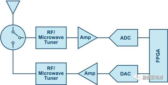
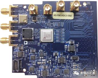
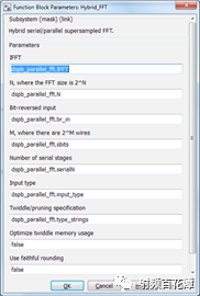
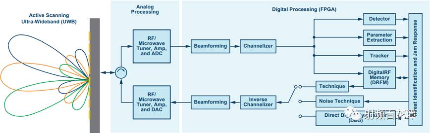 Figure 4. Block diagram of a general electronic warfare system