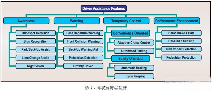
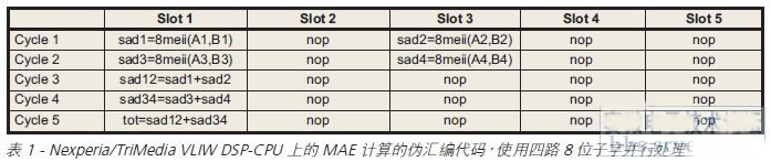
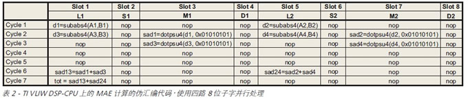
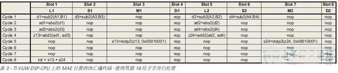
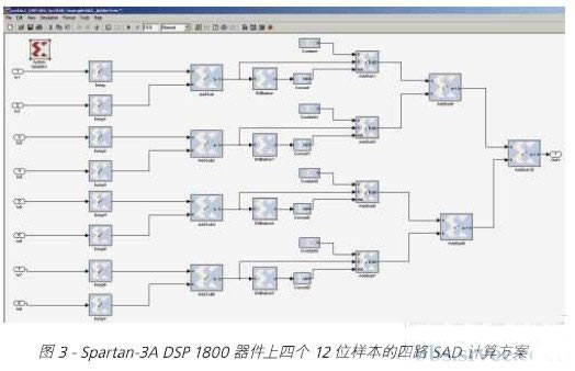
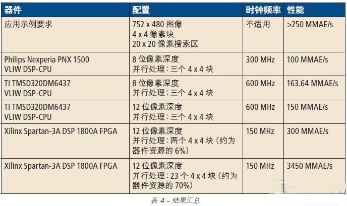
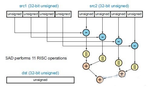
Automotive engineers use a variety of smart technologies to help people drive their cars safely. The main technologies in automotive systems include radar, ultrasound and camera/visual sensing. These technologies are collectively referred to as driver assistance (DA) systems for assisting safe driving in harsh conditions and hazardous road conditions. This article refers to the address: http:// The first generation of video DA systems is currently available in a variety of production vehicles. Most of these systems provide drivers with video images of the surroundings of the vehicle. The most common is the parking/reverse assist system, which uses a rear view camera to capture the scene behind the car and display images on the screen of the radio/navigation system or on a small display in the dashboard. The second-generation camera system is in the development and testing phase and is currently in limited use. The second generation system does not only provide images to the driver, but uses image processing and parsing to extract information from the video stream and characterize and evaluate the vehicle environment. The driver will receive a corresponding warning if necessary. As engineers gain practical experience in vehicle environmental characterization, future DA technologies will be more complex, providing consumers with more powerful utilities and enhancing the performance of other automotive subsystems. Figure 1 summarizes the various DA features available today and in the future. Advanced processing requirements The processing requirements of DA systems may exceed the capabilities of current automotive-grade serial DSP processors. In addition, in order to increase consumer value, the need to bundle multiple DA functions on a set of vision sensors is increasing. For example, a forward-looking vision module may need to support both lane departure warning, smart headlight control, and sign recognition, all of which require different processing algorithms. As a result, the DA market offers tangible opportunities for delivering system value through FPGAs with raw image data processing, configuration flexibility, and device scalability. The image processing and parsing functions of the visual DA system may include spatial/temporal filtering, lens distortion correction, image sharpening, contrast enhancement, edge detection, image matching, object recognition, and object tracking, and in some cases, graphic overlay. Of particular interest is an image matching function that supports motion estimation or stereo disparity calculation. To illustrate the performance value of FPGA processing, let's consider a vision system that produces a wide-format VGA resolution imaging device (752 x 480 pixels) at 30 Hz frame rate (fps) and estimates the motion of the object between frames (or flow). There is an algorithm (also applicable to stereo disparity calculation) that divides an image into several blocks (such as a size of 4 × 4 pixels), and then determines each image block in the first frame to the specified search area in the second frame (such as 20 × Matching condition for a position within 20 pixels). A commonly used matching condition is to find the minimum absolute error of pixel gray (MAE) between the 4×4 block in the first frame image and the pixel in the search area on the second frame image by the operator SAD (absolute difference sum). ). Our 4×4 block matching example requires performance above 250 MMAE/s (millions of MAE per second) because (752 pixels) × (480 rows) × (20 × 20 pixel search area) × (30 fps) / (4 × 4 pixel block size) = 270,720,000 MAE/s. MAE represents the final matching error of a 4×4 pixel block, while SAD refers to the sum of absolute differences calculated from four independent element pairs. Therefore, each SAE requires four SAD operations. Processing options Processing options determined by automotive design engineers include the Very Long Instruction Word (VLIW) DSP-CPU and FPGA. The processing power of an FPGA is much higher than any existing VLIW DSP-CPU. This is due to the FPGA architecture: a large number of parallel functional units (including programmable MAC) make FPGA performance 10-30 times better than any DSP (depending on the application implemented), even if the FPGA clock frequency is better than DSP- The clock frequency of the CPU is much lower. We use block matching arithmetic examples to demonstrate that Xilinx® FPGAs perform better than any VLIW DSP-CPU processor. SAD and MAE calculations in VLIW DSP-CPU processors The SAD operation of four 8-bit pixel video data units can be implemented in a 32-bit architecture single instruction multiple data (SIMD) DSP-CPU, so the operation equivalent to 11 basic instructions can be effectively executed in only one cycle. ,as shown in picture 2. figure 2 For example, the Nexperia PNX1500 media processor is equipped with a 32-bit TriMedia VLIW-CPU that can execute two four-way SAD instructions in one clock cycle for 8-bit pixels with two-cycle delay. Counting very long instruction words is up to five basic RISC/SIMD instructions per clock cycle, of which only two can be SAD instructions (called “8meii†in the TriMedia data sheet). Therefore, it takes five clock cycles to perform MAE calculation on a 4×4 block, as shown in Table 1: Two cycles are used for pipeline processing of two four-way SAD instructions (Cycle 1 is used for sad1/sad2, cycle 2) In sad3/sad4); three cycles are used for the accumulation of partial results (cycles 3, 4 and 5). Therefore, if only one block is processed, a 300 MHz Nexperia PNX1500 processor can handle up to 60 MMAE/s. If you process more than one 4×4 block at a time, the maximum performance can be slightly improved. For example, two parallel 4x4 blocks of MAE can be calculated in seven cycles, with a performance of 85.71 MMAE/s, while nine blocks are required to process three blocks, with a performance of 100 MMAE/s. The maximum number of blocks that can be processed in parallel is limited by the number of SIMD SAD operations allowed in any long instruction word, the number of general-purpose registers of the VLIW-CPU, and the scheduling algorithm of the optimizing compiler. If you continue to increase the number of blocks, the overall performance will tend to be saturated, so we consider no more than three MAEs for parallel processing. Texas Instruments' TISD320DM6437 digital media processor has a long instruction consisting of eight basic RISC operations per cycle, passing through two data paths, each with four time slots per cycle. The VLIW-CPU can execute up to two SAD instructions per cycle (referred to as “subabs4†in the TI DM6437 data sheet), with one cycle delay for each instruction. However, to accumulate partial results, a SIMD MAC operation with a three-cycle delay (called "dotpsu4") must be performed using the constant 0x01010101. Therefore, the 600 MHz TI DM6437 DSP-CPU can calculate a MAE in seven cycles (as shown in Table 2), so the maximum performance for a 4 x 4 pixel block is 85.71 MMAE/s. If two blocks are processed in parallel, nine cycles are required with a performance of 133.33 MMAE/s; while three blocks require 11 cycles with a performance of 163.64 MMAE/s, which is still below our 250 MSAD/s requirement. VLIW DSP-CPU is not performing well At this point, we have been assuming 8 bits per pixel, which is a good fit for 32-bit architecture DSP-CPU processors. However, the new CMOS image sensor has a higher resolution range of 12 to 14 bits per pixel. For these data types, the traditional four-way 8-bit subword SIMD of the 32-bit architecture is not efficient enough to be replaced with a dual 16-bit halfword SIMD with subword parallelism of only two. Therefore, since calculating a MAE requires more clock cycles, the maximum performance is greatly reduced. Table 3 shows the possible pseudo-assembly code for calculating the SAD using a 16-bit subword instruction on the TI VLIW DSP-CPU, assuming that the delay is correct and the function transmit time slot allows execution of such an instruction. Therefore, a 4x4 block requires eight cycles, while parallel processing of two and three blocks requires 10 and 12 cycles, respectively. At this time, the corresponding maximum performance is 75 MMAE / s, 120 MMAE / s and 150 MMAE / s. These numbers are smaller than those obtained using 8-bit subword instructions. SAD and MAE performance of Spartan-3A DSP FPGAs To fill the processing performance gap between SpartanTM-3 and VirtexTM-4 devices, Xilinx introduced the Spartan 3A-DSP 1800A and 3400A FPGAs. These devices incorporate a modified version of the DSP48 slice in Virtex-4 devices. In addition, 3A-DSP devices include a large amount of on-chip memory (Block RAM). These two enhancements combined with price points for a wide range of applications make 3A-DSP devices ideal for automotive vision DA systems. Figure 3 shows the four-way 12-bit pixel SAD calculation scheme on the Spartan-3A DSP 1800 (XC3SD1800A-4FG676) device. This implementation is done using the System Generator for DSP design flow (a digitally and cycle-precise synthesizable library in the Simulink tool provided by Xilinx). The required number of resources is 121 slices (236 LUTs and 140 triggers). Copy this structure four times and add partial results to get the entire 4×4 block calculation scheme, which requires 508 slices (990 triggers and 606 LUTs) with one cycle throughput (which means Calculate the new MAE from any clock cycle and seven cycle delays. If you use a 150 MHz clock frequency (the device has a maximum clock frequency of 250 MHz), you only need two parallel structures (about 6% of the device area) to achieve 300 MMAE/s performance to meet the 250 MMAE/ for the sample application. s performance requirements. This saves a lot of resources for other image processing functions, data routing pipelines, memory interface controllers, and a 32-bit MicroBlazeTM embedded processor for serial processing and external communication. For reference, still with 150 MHz, the Spartan 3A-DSP 1800A device can process up to 23 blocks in parallel (70% x 16,640 slices/508 slices/block = 23 blocks) using only 70% of the entire FPGA device. The highest performance corresponding to this is 3,529 MMAE/s, which is at least 25 times higher than the highest performance of the 600 MHz TI DSP-CPU. in conclusion Using automotive vision applications as an example, we illustrate how to use the programmable parallel processing power of medium-sized, low-cost Xilinx FPGAs to provide processing performance beyond the VLIW DSP-CPU. Table 4 lists our analysis results. Note that for a 4 x 4 block MAE calculation of 12-bit pixel data, the performance of the Spartan-3A DSP is only twice that of the TI TMS320DM6437 at a quarter clock speed. In addition, the FPGA's resource utilization is only 6%, so other image processing functions can be implemented on the same device (parallel processing can be adopted if necessary). On the other hand, the VLIW DSP-CPU is fully occupied during SAD calculations, consuming the available time slots of the serial processor long instructions, so there is very little opportunity to perform other functions simultaneously. Our estimated clock frequency for FPGAs is fairly conservative (150 MHz vs. 250 MHz), as is the search area for motion estimation (the larger the search area, the more MAEs need to be calculated). For example, a 30x30 search area requires 609 MMAE/s performance (far more than the VLIW DSP-CPU capability), while it only occupies 12% of the slice on the 1800A device. Finally, we did not use the DSP48 MAC unit at all when implementing MAE: we estimate that if four DSP48 units are used instead of an adder tree consisting of 100 slices, a 4×4 block of a 12-bit input data MAE will occupy 400. Slices (782 flip-flops and 400 LUTs) and four DSP48s. As a result, the Spartan-3A DSP 1800A device is ideal for vision applications that require extreme processing performance, flexibility and scalability, such as vision applications in future automotive driver assistance systems.
Desktop style 12v and 24v series can be used in many different electronics. EMC, LVD, FCC, RoHS are available in our company. OEM and ODM are available, samples are free for testing, all our products have 2 years warranty.
Our products built with input/output overvoltage protection, input/output overcurrent protection, over temperature protection, over power protection and short circuit protection. You can send more details of this product, so that we can offer best service to you!
Led Adapter, Lcd Adapter,Speaker Power Adapter,Lcd Power Supply Shenzhen Waweis Technology Co., Ltd. , https://www.waweisasdapter.com