If the frequency of the digital logic circuit reaches or exceeds 45 MHz to 50 MHz, and the circuit operating above this frequency already accounts for a certain amount (for example, 1/3) of the entire electronic system, it is usually called a high frequency circuit. High-frequency circuit design is a very complex design process, and its wiring is critical to the overall design! [first move] multi-layer board wiring High-frequency circuits tend to have high integration and high wiring density. The use of multi-layer boards is both necessary for wiring and an effective means to reduce interference. In the PCB Layout stage, a reasonable selection of the printed board size of a certain number of layers can make full use of the intermediate layer to set the shielding, better achieve the near grounding, and effectively reduce the parasitic inductance and shorten the transmission length of the signal, and at the same time All of these methods are advantageous for the reliability of high frequency circuits by reducing the crosstalk of signals, etc. in magnitude. According to the data, the four-layer board is 20dB lower than the noise of the double-panel. However, there is also a problem. The higher the PCB half-layer number, the more complicated the manufacturing process and the higher the unit cost. This requires us to select the appropriate number of PCB boards for PCB layout. Proper component layout planning and proper routing rules to complete the design. [Second measure] The less the lead between the high-speed electronic device pins is bent, the better. The lead wire of the high-frequency circuit wiring is preferably a full line, which needs to be turned, and can be folded by a 45-degree line or a circular arc. This requirement is only used to improve the fixing strength of the copper foil in the low-frequency circuit, and in the high-frequency circuit, the content is satisfied. One requirement is to reduce the external transmission and mutual coupling of high frequency signals. [Third measure] The shorter the lead between the pins of the high-frequency circuit device, the better. The radiant intensity of the signal is proportional to the length of the trace of the signal line. The longer the high-frequency signal lead, the easier it is to couple to the component close to it, so for clocks such as signals, crystals, DDR data, High-frequency signal lines such as LVDS lines, USB lines, and HDMI lines are required to be as short as possible. [Fourth trick] The less the number of lead layers between the pins of the high-frequency circuit device, the better. The so-called "the least alternating between the layers of the leads is better" means that the fewer vias (Via) used in the component connection process, the better. According to the side, a via can bring about a distributed capacitance of about 0.5pF, and reducing the number of vias can significantly increase the speed and reduce the possibility of data errors. [Fifth trick] Pay attention to the "crosstalk" introduced by the parallel lines of the signal lines. High-frequency circuit wiring should pay attention to the "crosstalk" introduced by the parallel lines of the signal lines. Crosstalk refers to the coupling phenomenon between signal lines that are not directly connected. Since the high-frequency signal is transmitted along the transmission line in the form of electromagnetic waves, the signal line acts as an antenna, and the energy of the electromagnetic field is emitted around the transmission line, and an undesired noise signal generated by the mutual coupling of the electromagnetic fields between the signals is generated. Called Crosstalk. The parameters of the PCB layer, the spacing of the signal lines, the electrical characteristics of the driver and receiver, and the termination of the signal line all have a certain impact on crosstalk. Therefore, in order to reduce the crosstalk of high-frequency signals, it is required to do the following as much as possible during wiring: Inserting a ground or ground plane between two lines with severe crosstalk can allow isolation and reduce crosstalk under the conditions allowed by the wiring space. When there is a time-varying electromagnetic field in the space around the signal line, if parallel distribution cannot be avoided, a large area "ground" can be placed on the reverse side of the parallel signal line to greatly reduce the interference. Under the premise of wiring space permission, increase the spacing between adjacent signal lines, reduce the parallel length of the signal lines, and the clock lines should be perpendicular to the key signal lines and not parallel. If the parallel traces in the same layer are almost unavoidable, in the adjacent two layers, the direction of the traces must be perpendicular to each other. In digital circuits, the usual clock signals are signals whose edges change rapidly, and the external crosstalk is large. Therefore, in the design, the clock line should be surrounded by ground lines and more ground holes to reduce the distributed capacitance, thus reducing crosstalk. For high-frequency signal clocks, use low-voltage differential clock signals as much as possible and cover the ground. You need to pay attention to the integrity of the package. Do not leave the unused input terminal, but ground it or connect it to the power supply (the power supply is also ground in the high-frequency signal loop). Because the suspended line may be equivalent to the transmitting antenna, grounding can suppress the emission. Practice has proved that using this method to eliminate crosstalk can sometimes be effective immediately. [Sixth move] the power supply pin of the integrated circuit block increases the high frequency untwisting capacitance A high frequency untwisting capacitor is added to the power supply pin of each integrated circuit block. Increasing the high frequency decoupling capacitor of the power supply pin can effectively suppress the high frequency harmonics on the power supply pin to form interference. [Seventh trick] The ground of the high-frequency digital signal is isolated from the analog signal ground. When the analog ground wire, digital ground wire, etc. are connected to the common ground wire, the high-frequency turbulent magnetic beads are used to connect or directly isolate and select a suitable place for single-point interconnection. The ground potential of the ground of the high-frequency digital signal is generally inconsistent. There is often a certain voltage difference between the two directly. Moreover, the ground of the high-frequency digital signal often has a very rich harmonic component of the high-frequency signal. When the digital signal ground and the analog signal ground are directly connected, the harmonics of the high-frequency signal interfere with the analog signal by means of ground-line coupling. Therefore, in general, the ground of the high-frequency digital signal and the ground of the analog signal are to be isolated, and a single-point interconnection at a suitable position or a high-frequency turbulent magnetic bead interconnection may be employed. [eighth trick] avoid loops formed by traces Do not form a loop as much as possible for all types of high-frequency signal traces. If it is unavoidable, make the loop area as small as possible. [Ninth move] must ensure good signal impedance matching During the transmission of the signal, when the impedance does not match, the signal will reflect in the transmission channel, and the reflection will overshoot the composite signal, causing the signal to fluctuate around the logic threshold. The fundamental way to eliminate the reflection is to make the impedance of the transmitted signal match well. Since the difference between the load impedance and the characteristic impedance of the transmission line is larger, the reflection is also larger. Therefore, the characteristic impedance of the signal transmission line should be equal to the load impedance as much as possible. At the same time, it should be noted that the transmission line on the PCB should not be abrupt or corner, try to keep the impedance of each point of the transmission line continuous, otherwise there will be reflection between the segments of the transmission line. This requires the following wiring rules to be observed when performing high-speed PCB routing: USB wiring rules. USB signal differential routing is required. The line width is 10 mils, the line spacing is 6 mils, and the ground and signal lines are 6 mils apart. HDMI wiring rules. HDMI signal differential routing is required, with a linewidth of 10 mils and a line spacing of 6 mils. The spacing between each pair of HDMI differential signal pairs exceeds 20 mils. LVDS wiring rules. Requires LVDS signal differential trace, line width 7mil, line spacing 6mil, the purpose is to control the differential signal impedance of HDMI to 100+-15% ohms DDR wiring rules. DDR1 routing requires that the signal not go through the hole as much as possible, the signal line is equal, the line is equidistant from the line, the line must meet the 2W principle to reduce the crosstalk between signals, and the high-speed data for DDR2 and above requires high-frequency data. The lines are equal in length to ensure impedance matching of the signals. [Tenth move] to maintain the integrity of signal transmission Maintain the integrity of signal transmission and prevent "ground bounce" caused by ground segmentation. The PCB is the printed circuit board, which is the carrier of the electronic circuit. At the same time, it is also the last link of the circuit design. In today's electronic products, the internal structure is used to the PCB. PCB is so important, how should we systematically and systematically learn PCB printed board design? Many people want to participate in offline training courses, but thousands of training costs are astounding, and they want to learn PCB design quickly through self-study, but based on the special nature of PCB design, and on the network. There are few, systematic and comprehensive PCB design courses, and the content of the study is illegible and cannot be applied to specific practical projects. In order to help everyone better, faster and systematically master the core knowledge of PCB design, E-Commerce College and Lin Chaowen team carefully designed the PCB design quick start series course, aiming at providing a lot of beginners and engineers who are keen on PCB manufacturing. Good system and scientific learning PCB design opportunities! In the field of hardware interconnection design, Mr. Lin has more than ten years of management experience in PCB. Proficient in Cadence, Mentor, PADS, AD, HyperLynx and other PCB design simulation tools, long-term leadership team to tackle military and communications, communications and other high-tech design simulation projects. Published many EDA books, a series of books by the industry called "high-speed PCB design collection." For the first time, the PCB design course adopted online live broadcast. This is the first time that Mr. Lin Chaowen has launched a series of PCB design courses on the Internet platform. (Tonight at 8:00, Lin Chaowen will be the third live broadcast of PCB design -> Click here to listen to the live broadcast ) The PCB design course focuses on practical hands and reduces the theoretical part. Each course will be demonstrated by video live broadcast. The course covers the whole process node of high-speed PCB design. The course content is detailed and detailed, and with a number of practical cases, so that the learning process will not be boring, knowledge point technology implementation is easy to understand. This course is an introduction to PCB design: Lin Chaowen takes you to the basics of PCB design. After completing this course, you will gain the following skills: 1. Master the PADS Logic schematic design 2, master OrCAD schematic design 3. Master PADS Logic component library management 4, master the OrCAD principle library management 5, master the schematic output related data 6, understand the complete process of PCB design 7, master PADS Layout PCB design knowledge 8, familiar with PADS Router practical application skills 9, master the PADS output production file Registration address: http://t.elecfans.com/topic/22.html?elecfans_trackid=pctopline Course registration: 1. This course is a pre-sale course. The first registration is limited to 200 people, and the pre-sale price is 199 yuan. 2. Registration time: October 11, 2017 - November 11, 2017 3. This course is an online live course, officially started on October 11th, and broadcasts twice a week; 4. After purchasing the course, please be sure to join the exclusive QQ group of students. Please add the name of the enthusiast to the group, such as: “Enthusiast User xxx†Two times a week online live + offline high-intensity learning + phased learning tasks + live Q & A, to help you familiarize yourself with the knowledge framework, project skills and practical methods required for a complete system of PCB design engineers!
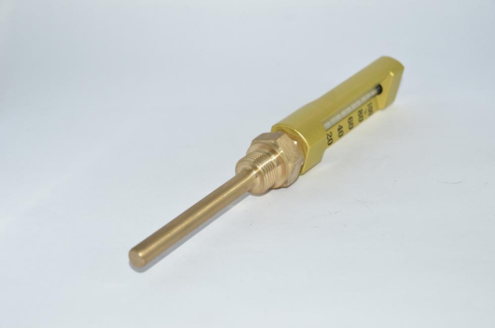
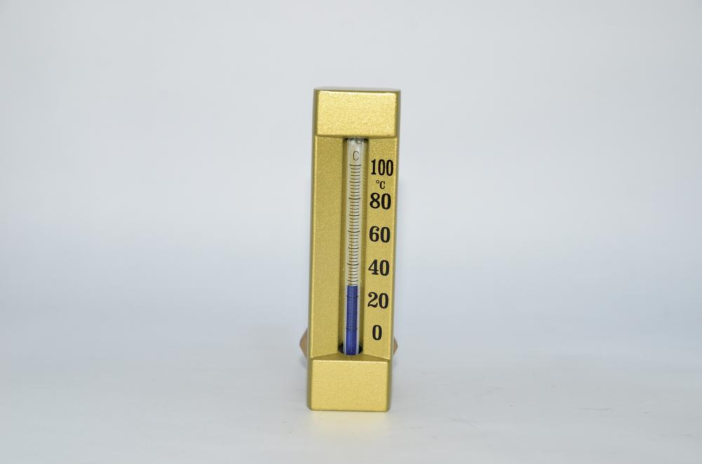
Marine thermometers include wlg-421 and wlg-422 models.A thermometer of 0 ℃ angle straight type with a parting gauge for ship shape. The upper body is made of gold and the surface is gold.
Marine mold external standard, V-shape, shape parting and 90 ℃ angle spacing. The upper body is made of aluminum and gold is formed by grinding wheel or sand blasting. The length of the upper body of the thermometer: 110mm, 150mm and 200mm· Glass feeling: round or round φ 7 ~ 7.5mm, within - 40 ℃ ~ 200 ℃ / - 40 ℃ ~ 40 ℃ 0 ℉, marine blue or organic temperature liquid, amber color filled with transparent thermometer (below 400 ℃ / 750 ℉); Above 200 ℃ / 400 ℉, filled with mercury in ℉, above 400 ℃ / 750 ℉
Marine Thermometer,Marine Industrial Thermometer Measurement,Brass Marine Thermometer,Industrial Marine Digital Thermometer Taizhou Jiabo Instrument Technology Co., Ltd. , https://www.taizhoujbcbyq.com

Sweep and sign up for the course immediately! 
