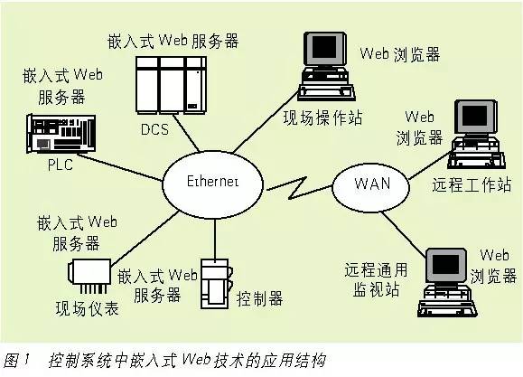
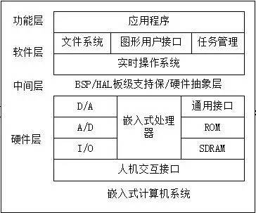
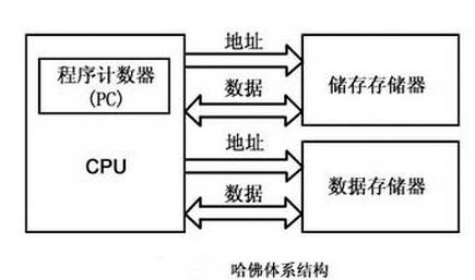
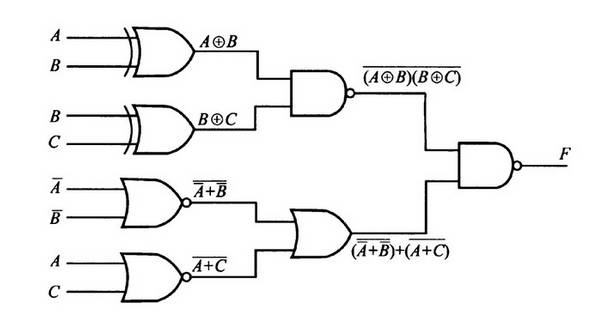
1. What is embedded? IEEE (Institute of Electrical and Electronics Engineers) defines embedded systems: "Devices for controlling, monitoring, or assisting in the operation of machines and equipment." Originally: Devices Used to Control, Monitor or Assist the Operation of Equipment, Machinery or Plants). An embedded system is a specialized computer system that is part of a device or device. Typically, an embedded system is an embedded processor control board in which the control program is stored in ROM. In fact, all devices with digital interfaces, such as watches, microwave ovens, video recorders, and automobiles, use embedded systems. Some embedded systems also include an operating system, but most embedded systems implement full control from a single program. logic. Defined from the application object, the embedded system is a combination of software and hardware, and can also cover auxiliary devices such as machinery. The embedded system generally recognized in China is defined as: application-centered, computer-based, software and hardware tailored to meet the strict requirements of the application system for functions, reliability, cost, size, power consumption and other special computer systems. An embedded system device generally consists of an embedded computer system and an execution device. The embedded computer system is the core of the entire embedded system, and is composed of a hardware layer, an intermediate layer, a system software layer, and an application software layer. The execution device, also known as the controlled object, can accept control commands issued by the embedded computer system to perform the specified operations or tasks. The actuator can be very simple, such as a tiny motor on the phone, which is turned on when the phone is in vibration receiving state; it can also be complicated, such as the SONY smart robot dog, which integrates multiple micro-small control motors and various sensors. Thereby, various complicated actions and various state information can be performed. 2, the composition of the embedded system First, the hardware layer The hardware layer includes an embedded microprocessor, memory (SDRAM, ROM, Flash, etc.), general device interface, and I/O interface (A/D, D/A, I/O, etc.). Adding a power circuit, a clock circuit and a memory circuit based on an embedded processor constitutes an embedded core control module. The operating system and applications can be hardened in ROM. Second, the intermediate layer between the hardware layer and the software layer is the middle layer, also known as the Hardware Abstract Layer (HAL) or the Board Support Package (BSP). The semi-system upper layer software is separated from the underlying hardware. Open, so that the underlying driver of the system is independent of the hardware, the upper software developers do not need to care about the specific conditions of the underlying hardware, and can be developed according to the interface provided by the BSP layer. This layer typically contains initialization of the underlying hardware, input/output operations of the data, and configuration capabilities of the hardware device. In fact, BSP is a layer of software between the operating system and the underlying hardware, including most of the hardware modules in the system that are closely related to the hardware. Designing a complete BSP requires two parts of the work: the BSP function of the hardware initialization of the embedded system, and the design of the hardware-related device driver. Third, the system software layer The system software layer consists of real-time multi-tasking operating system (RTOS), file system, graphical user interface (GUI), network system and general component modules. RTOS is the foundation and development platform for embedded applications. 3, real-time system (1) Definition: A system that can perform system functions and respond to external or internal, synchronous or asynchronous time within a specified or determined time. (2) Difference: The general system generally pursues the average response time of the system and the user's convenience; while the real-time system mainly considers the system behavior in the worst case. (3) Features: time constraint, predictability, reliability, and interaction with the external environment. (4) Hard real-time (strong real-time): It means that the time requirement of the application should be fully satisfied, otherwise it will cause major security accidents and even cause major loss of life and property and ecological damage, such as: aerospace and military. (5) Soft real-time (weak real-time): Although some applications have time requirements, real-time tasks occasionally violate this requirement and will not have serious impact on system operation and environment, such as monitoring system and real-time information collection system. (6) Task constraints include: time constraints, resource constraints, execution order constraints, and performance constraints. 5, real-time system scheduling (1) Scheduling: Given a set of real-time tasks and system resources, determine the entire process of when and where each task is executed. (2) Preemptive scheduling: usually priority-driven scheduling, such as uCOS. The advantage is that the real-time performance is good, the response is fast, the scheduling algorithm is relatively simple, and the time constraint of the high-priority task can be guaranteed; the disadvantage is that there are many context switches. (3) Non-preemptive scheduling: Usually scheduled by time slice, the task is not allowed to be interrupted during execution. Once the task occupies the processor, it must be executed or voluntarily given up, such as WinCE. The advantage is that the context switching is less; the disadvantage is that the processor has low effective resource utilization and poor schedulability. (4) Static table driving strategy: Before the system runs, according to the time constraints and associations of each task, a certain search strategy is used to generate a running time table, indicating the starting running time and running time of each task. (5) Priority driving strategy: Determine the execution order of tasks according to the priority of the task. (6) Real-time task classification: periodic tasks, incidental tasks, and non-periodic tasks. (7) General structure model of real-time system: data collection task realizes sensor data collection, data processing task processes the collected data, and sends the processed data to the execution organization management task control organization for execution. 5, embedded microprocessor architecture (1) von Neumann structure: program and data share a storage space, program instruction storage address and data storage address point to different physical locations of the same memory, using a single address and data bus, the program and data have the same width. For example: 8086, ARM7, MIPS... (2) Harvard structure: Program and data are two independent memories. Each memory is independently addressed and accessed independently. It is a memory structure that separates program storage from data storage. For example: AVR, ARM9, ARM10... (3) Comparison of CISC and RISC features. The time P required by the computer to execute the program can be calculated by the following formula: P = I × CPI × T I: The number of instructions that are run on the machine after the high-level language program is compiled. CPI: The average number of cycles required to execute each instruction. T: The time of each machine cycle. (4) The idea of ​​the pipeline: Sub-processes in which the serial execution of an instruction is changed into several instructions in the CPU are executed in the CPU. (5) Index of the pipeline: throughput rate: the number of results of the pipeline processor in unit time. If the sub-process of the pipeline takes a different amount of time, the throughput rate should be the reciprocal of the longest sub-process. Settling time: The time at which the pipeline starts working to reach the maximum throughput rate. If the time used by m sub-processes is the same, both are t, then the time T=mt is established. (6) Byte order of information storage A, memory unit: byte (8 bits) B. The word length determines the addressing capability of the microprocessor, that is, the size of the virtual address space. C, 32-bit microprocessor virtual address space bit 232, which is 4GB. D, little endian byte order: the low byte is at the low address of the memory, and the high byte is at the high address of the memory. E, big endian byte order: the high byte is at the low address of the memory, and the low byte is at the high address of the memory. F. The storage order of network devices depends on the data link layer in the bottom layer of the OSI model. 6, the logic circuit foundation (1) According to whether the circuit has a storage function, the logic circuit is divided into: a combinational logic circuit and a sequential logic circuit. (2) Combinational logic circuit: The output of the circuit at any time depends only on the input signal at that moment, regardless of the state of the circuit before the input signal is applied. Commonly used logic circuits include decoders and multiplexers. (3) Sequential logic circuit: The output of the circuit at any time is not only related to the input at that moment, but also related to the state of the circuit at that moment. Therefore, memory elements must be included in the sequential circuit. Triggers are the basis for constructing sequential logic circuits. Commonly used sequential logic circuits include registers and counters. (4) The concept of truth table, Boolean algebra, Morgan's law, and gate circuit. (5) NOR (or non-) and NAND (NAND) gates are called full-featured gates and can implement any kind of logic function. (6) Decoder: A combined logic network with multiple inputs and multiple outputs. Each time an n-bit binary code is entered, at most one of the m outputs is valid. When m=2n is, it is fully decoded; when m is 2n, it is partially decoded. (7) Since the high-level output current of the integrated circuit is small, and the low-level output current is relatively large, when the integrated gate circuit directly drives the LED, the low-level driving mode is often used. The liquid crystal seven-segment display LCD utilizes different optical characteristics of the liquid crystal with an applied electric field and no external electric field to display characters. (8) The clock signal is the basis of the timing logic and is used to determine the appropriate update of the state in the logic unit. Synchronization is the main constraint in clock control systems. (9) When selecting a trigger, the trigger mode is a factor that must be considered. There are two trigger modes: Mode 1: Level trigger mode: It has a simple structure and is often used to form a scratchpad. Mode 2: Edge trigger mode: It has strong anti-data interference capability and is commonly used to form registers, counters, etc. 7, bus circuit and signal drive (1) The bus is a collection of various signal lines and is a common path for transferring data, addresses, and control information between components in an embedded system. At the same time, one binary signal can be transmitted on each path. According to the type of information transmitted by the bus, it can be divided into: data bus (DB), address bus (AB) and control bus (CB). (2) Main parameters of the bus: Bus bandwidth: The amount of data that can be transmitted on the bus within a certain period of time, generally expressed in MByte/s. Bus width: The number of bits of data that the bus can transmit at the same time, that is, the concept of bus widths such as 32-bit and 64-bit, which is often referred to as bus width. The wider the bit width of the bus, the larger the data transfer rate per second of the bus, that is, the wider the bus bandwidth. Bus frequency: The working clock frequency is in MHz. The higher the operating frequency, the faster the bus operates, that is, the wider the bus bandwidth. Bus bandwidth = bus bit width x bus frequency / 8, in MBps. Common bus: ISA bus, PCI bus, IIC bus, SPI bus, PC104 bus and CAN bus. (3) Only devices with three-state outputs can be connected to the data bus. The commonly used tri-state gates are output buffers. (4) When the load connected to the bus exceeds the load capacity of the bus, a buffer or driver must be added between the bus and the load. The most commonly used is a tristate buffer, which functions to drive and isolate. (5) The bus bus multiplexing technology can realize the sharing of the data bus and the address bus. But it will bring two problems: A. It is necessary to add an external circuit to multiplex and decouple the bus signal, for example: address latch. B. The bus speed is lower than that of the non-multiplexed bus system. (6) Two types of bus communication protocols: synchronous mode and asynchronous mode. (7) The solution to the bus arbitration problem is based on the concept of priority (priority). 8, level conversion circuit (1) Digital integrated circuits can be divided into two categories: bipolar integrated circuits (TTL) and metal oxide semiconductors (MOS). (2) CMOS circuits are widely used due to their extremely low static power consumption, high operating speed and strong anti-interference ability. (3) The solution to the TTL and CMOS circuit interface is to connect a pull-up resistor R between the output of the TTL circuit and the power supply. The value of the pull-up resistor R is determined by the high-level output leakage current IOH of the TTL. The TTL should use a different R value. 9, information representation and computing basis in embedded systems (1) Carry count system and conversion: This is relatively simple, and you should also know how to convert, and there is a possibility of a problem. (2) Representation of numbers in computers: source code, inverse code and complement code. The inverse of the positive number is the same as the source code. The inverse of the negative number is the source code of the number except the sign bit. The complement of a positive number is the same as the source code, and the complement of a negative number is one plus the inverse of the number. For example, the source code B of -98 is B-complement B (3) fixed-point notation: the position of the decimal point of the number is fixed by the artificial agreement. Floating point notation: The decimal point position of a number is floating, which consists of a mantissa part and an order part. Any binary N can always be written as: N=2P×S. S is the mantissa and P is the order. (4) Chinese character representation, to understand the transformation of GB2318-80 Chinese code and internal code. (5) Waveform quantization parameters in speech coding (may be a simple calculation problem) Sampling frequency: The number of samples in one second, reflecting the interval between sampling points. The upper limit of the human ear is 20 kHz, so the sampling frequency above 40 kHz is enough to satisfy. The sampling frequency used for CD recording is 44.1 kHz. Measurement accuracy: The quantization level of the sample. Currently, the standard sampling level has 8 bits and 16 bits. Number of channels: mono and stereo dual channels. Stereo requires twice the storage space. 10, error control coding (1) According to the function of the code group, it can be divided into two types: error detection code and error correction code. The error detection code refers to a code that can automatically detect an error, such as a parity check code; an error correction code refers to a code that can not only detect an error but also automatically correct an error, such as a cyclic redundancy check code. (2) Parity check code, Hamming code, cyclic redundancy check code (CRC). 11. Error control coding metrics for embedded systems (1) Performance indicators: divided into component performance indicators and comprehensive performance indicators, including: throughput, real-time and various utilization. (2) Reliability and safety Reliability is the most important and outstanding basic requirement of embedded systems. It is a guarantee that an embedded system can work normally. It is generally measured by the mean time between failures (MTBF). (3) Maintainability: Generally expressed by the average repair time MTTR. (4) Availability (5) Power consumption (6) Environmental adaptability (7) Universality (8) Security (9) Confidentiality (10) Scalability The price in the price/performance ratio, in addition to the price of the direct purchase of the embedded system, should also include installation costs, several years. Operating maintenance costs and software rental fees. Evaluation methods for embedded systems: measurement methods and model methods (1) Measurement is the most direct and basic method, and two problems need to be solved: A. Determine the system parameters to be measured according to the purpose of the study. B. Choose the tools and methods of measurement. (2) There are two ways to measure: sampling mode and event tracking mode. (3) The model method is divided into an analysis model method and a simulation model method. The analytical model method uses some mathematical equations to describe the model of the system. The simulation model method uses the operation of the simulation program to dynamically express the state of the embedded system, and performs systematic statistical analysis to obtain performance indicators. (4) The most used in the analytical model method is the queuing model, which consists of three parts: input stream, queuing rules, and service organization. (5) Using the model to evaluate the system requires solving three problems: designing the model, solving the model, and calibrating and validating the model. 12, interface technology 1, Flash memory (1) Flash memory is a kind of non-volatile memory, which can be divided into NOR Flash and NAND Flash according to different structures. (2) Features of Flash memory: A. Block structure: It is physically divided into several blocks, and the blocks are independent of each other. B. First erase and write: Flash write operation can only write data bits from 1 to 0, and cannot write from 0 to 1, so you must perform an erase operation before initializing the memory to initialize the pre-written data bits. Is 1. The smallest unit of erase operation is a block, not a single byte. C. Operation instruction: To perform a write operation, it must input a string of special instructions (NOR Flash) or complete a timing (NAND Flash) to write data. D. Bit reversal: Due to the inherent characteristics of Flash, one or more data errors are occasionally generated during the reading and writing process. Bit reversal cannot be avoided, and the results can only be processed afterwards by other means. E. Bad block: Once the block is damaged, it will not be repaired. The result of a corrupted block operation is unpredictable. (3) Features of NOR Flash: The application can run directly in flash without having to read the code into system RAM. NOR Flash has a very high transmission efficiency and is very cost effective in the small capacity of 1MB~4MB, but the low write and erase speed greatly affects its performance. (4) Features of NAND Flash The ability to increase extremely high density cells allows for high storage densities and fast write and erase speeds, which is why all U-disks use NAND Flash as the storage medium. The difficulty with applying NAND Flash is that flash requires a special system interface. (5) The difference between NOR Flash and NAND Flash: A, NOR Flash read speed is slightly faster than NAND Flash. B, NAND Flash erase and write speed is much faster than NOR Flash C, NAND Flash has a poor random reading capability and is suitable for continuous reading of large amounts of data. D, NOR Flash with SRAM interface, with enough address introduction to address, you can easily access every byte inside it. NAND Flash's address, data, and commands share an 8-bit bus (16-bit products are written by the company), and each time it is read or written, it uses a complex I/O interface to serially access data. E, NOR Flash capacity is generally small, usually between 1MB ~ 8MB; NAND Flash is only used in products above 8MB. Therefore, NOR Flash is only suitable for data storage as long as it is applied to code storage media. F, the maximum number of erasures per block in NAND Flash is one million, and NOR Flash is 100,000 times. G, NOR Flash can be connected like other memory, very directly used, and can run code directly on it; NAND Flash requires special I/O interface, you must write the driver before you can continue to execute other operating. Because designers can never write to bad blocks, this means that virtual images must be made on NAND Flash from start to finish. H, NOR Flash is used for code storage, communication products, network processing and other fields that require high data reliability, and is used as code flash memory; NAND Flash is used for MP3, memory card, U disk, etc. with high storage capacity requirements. The domain is becoming a data flash. 2, RAM memory (1) Features of SRAM: SRAM stands for Static Random Access Memory. It maintains a value as long as it is powered. It has no refresh cycle. The flip-flop constitutes a basic unit with low integration. Each SRAM memory cell consists of 6 transistors, so its cost is high. It has a higher rate and is commonly used in cache memories. Usually SRAM has 4 types of pins: CE: Chip select signal, active low. R/W: Read and write control signals. ADDRESS: A set of address lines. DATA: A set of bidirectional signal lines for data transmission. (2) Features of DRAM: DRAM stands for Dynamic Random Access Memory. This is a semiconductor memory that is stored in the form of a charge. Each of its memory cells consists of a transistor and a capacitor, and the data is stored in a capacitor. Capacitors can lose charge due to leakage, and DRAM devices are unstable. It must be refreshed regularly to store the data in memory. The interface of DRAM is more complicated, usually with the following pins: CE: Chip select signal, active low. R/W: Read and write control signals. RAS: Row address strobe signal, usually connected to the upper part of the address. CAS: Column address strobe signal, usually connected to the lower part of the address. ADDRESS: A set of address lines. DATA: A set of bidirectional signal lines for data transmission. (3) Features of SDRAM: SDRAM stands for Synchronous Dynamic Random Access Memory. Synchronization means that the memory work requires a synchronous clock. The internal command transmission and data transmission are based on it. Dynamic means that the memory array needs constant refresh to ensure data is not lost. It usually only works at 133MHz. (4) Features of DDRAM DDRAM stands for Double Rate Synchronous Dynamic Random Access Memory (DDR), also known as DDR. DDRAM is based on SDRAM technology. SDRAM transmits data only once in one clock cycle. It transmits data during the rising period of the clock. DDR memory transfers data twice in one clock cycle. It can rise in the clock. Data is transmitted once for each period and period. At 133MHz, the DDR memory bandwidth can reach 133×64b/8×2=2.1GB/s. 3, hard disk, CD, CF card, SD card 4, GPIO principle and structure GPIO is the most basic form of I/O, it is a set of input or output pins. Some GPIO pins can be programmed to change the direction of operation. There are usually two control registers: the data register and the data direction register. The data direction register sets the direction of the port. If the pin is set to an output, the data register will control the state of that pin. If the pin is set as an input, the state of this input pin is controlled by the logic circuit layer on the pin. 5, A / D interface (1) The A/D converter is a circuit that converts an electrical analog quantity into a digital quantity. There are many ways to implement A/D conversion. The commonly used methods are counting method, double integral method and successive pushing method. (2) Counting A/D conversion method The main components of the circuit include: comparators, counters, D/A converters and standard voltage sources. The working principle is simply that there is a counter that increments from 0 and increments by one. Each time it is incremented by 1, the value is used as the input of the D/A converter, which produces a comparison voltage VO compared with the input analog voltage VIN. . If VO is less than VIN, continue to increment by 1 until VO is greater than VIN. At this time, the accumulated value of the counter is the output value of the A/D converter. This conversion method is characterized by simplicity, but at a slower speed, especially when the analog voltage is higher, the conversion speed is slower. For example, for an 8-bit A/D converter, if the input analog value is the maximum value, the counter should count from 0 to 255, and do 255 D/A conversion and voltage comparison to complete the conversion. (3) Double integral A/D conversion method The main components of the circuit include: an integrator, a comparator, a counter, and a standard voltage source. The working principle is that, firstly, the circuit integrates the input voltage to be measured for a fixed time, and then converts to the standard voltage to perform the reverse integration of the fixed slope, and the reverse integration proceeds to a certain time, and then returns to the starting value. Due to the fixed slope, the time to reverse integration of the standard voltage is proportional to the input analog voltage value. The larger the input analog voltage, the longer the reverse integration back to the start value. As long as the time taken for the reverse integration is measured by a standard high-frequency clock pulse, the digital quantity corresponding to the input analog voltage can be obtained, and the A/D conversion is completed. Its characteristic is that it has strong resistance to power frequency interference, high conversion precision, but slow conversion speed, usually the conversion frequency is less than 10Hz, mainly used for digital test instruments, temperature measurement and so on. (4) Successive approximation A/D conversion method The main components of the circuit include: a comparator, a D/A converter, a successive approximation register, and a reference voltage source. The working principle is that it is essentially the binary search method, and the principle of peacetime balance is the same. In the A/D conversion, the D/A converter increases the number of conversion bits bit by bit from high to low, generates different output voltages, and compares the input voltage with the output voltage. First, the highest bit is set to 1, which is equivalent to 1/2 of the reference voltage to be compared with the input voltage. If the input voltage is less than 1/2 of the reference voltage, the highest position is 0, otherwise it is set to 1. After that, the second highest position is 1, which is equivalent to a binary search in the range of 1/2, and so on, successive approximation. Its characteristics are fast speed and high conversion precision. It only needs M clock pulses for the N-bit A/D converter. It can be used to measure the transition process from tens to hundreds of microseconds. A common method of conversion. (5) Important indicators of A/D conversion (possibly taking some simple calculations) A. Resolution: Reflects the ability of the A/D converter to respond to small changes in input, usually expressed as the level of the analog voltage corresponding to the lowest bit of the digital output (LSB). The n-bit A/D converter can reflect the analog input level of 1/2n full scale. B. Range: The range of analog input voltages that can be converted is divided into unipolar and bipolar types. C. Conversion time: The time required to complete an A/D conversion, and the reciprocal is the conversion rate. D. Accuracy: Accuracy and resolution are two different concepts. Even if the resolution is high, the accuracy may not be high enough due to temperature drift, linearity, and the like. Accuracy has two representations of absolute precision and relative precision. The absolute accuracy is usually expressed in terms of the fractional value of the least significant bit LSB of the digital quantity, and the relative accuracy is expressed by the percentage of its analog voltage full scale. For example, a full-scale 10V, 10-bit A/D chip, if its absolute accuracy is ±1/2LSB, the quantization unit of its least significant bit LSB is: 10/1024=9.77mv, and its absolute accuracy is 9.77mv/2= 4.88mv, the relative accuracy is: 0.048%. 6, D / A interface basic (1) The D/A converter converts the digital quantity into an analog quantity. (2) In an integrated circuit, a T-type network is usually used to convert a digital quantity into an analog current, and an operational amplifier converts the analog circuit into an analog voltage. Performing D/A conversion actually requires the above two links. (3) Classification of D/A converters: A, voltage output type: often used as a high-speed D / A converter. B, current output type: generally used in external operational amplifiers. C. Multiplication type: can be used as a modulator and digitally attenuate the input signal. (4) Main indicators of D/A converter: resolution, setup time, linearity, conversion accuracy, temperature coefficient. 7, keyboard interface (1) Two forms of keyboard: linear keyboard and matrix keyboard. (2) There are usually two methods for identifying the close button on the keyboard: line scan and line inversion. (3) Line scanning method is a commonly used identification method for matrix keyboard keys. This method is divided into two steps: A. Identify which column of the keyboard is pressed: Make all the line lines low, and check if the line level of each column is low. If there is a column line low, it means that the button is pressed, otherwise Description No button press. B. If a column has a button press, identify which row of the keyboard is pressed: set the low level line by line, and set the remaining behaviors to be high level, query the changes of each column, if the column level becomes low level, You can then confirm that the button at the intersection of this column is pressed. 8, display interface (1) The basic principle of LCD is to control the passage of light by powering different liquid crystal cells to achieve the purpose of display. (2) There are two ways to provide light source for LCD: projection type and reflection type. The LCD display of the notebook computer is a projection type, and there is a light source behind the screen, so the external environment can eliminate the need for a light source. Generally, the LCD used on the microcontroller is reflective, requiring external power supply and working by reflected light. Electroluminescence (EL) is one way in which a liquid crystal panel provides a light source. (3) According to the classification of liquid crystal driving methods, common LCDs can be classified into three types: twisted nematic (TN), super twisted nematic (STN), and thin film transistor (TFT). (4) There are two types of LCDs available on the market: LCD display modules with drive circuits, as long as the bus mode is driven; LCD displays without drive circuits, using the controller scan mode. (5) Generally, when the LCD controller is working, the data of the specified address (display buffer) in the SDRAM is directly read by the SDRAM controller through the DMA request bus, and the data is converted into the LCD scan data format by the LCD controller. Directly drive the LCD display. (6) The VGA interface is essentially an analog interface, generally adopting a unified 15-pin interface, including 2 NC signals, 3 display data buses, 5 GND signals, 3 RGB color components, and 1 line sync signal. And 1 field sync signal. The level standard used for its color component is the RS343 standard defined by EIA. 9, touch screen interface (1) According to the working principle, the touch screen can be divided into: surface acoustic wave screen, capacitive screen, resistive screen and infrared screen. (2) The touch screen is controlled by a professional chip such as the ADS7843. 10, audio interface (1) Basic principle: The data input by the microphone is decoded by the audio codec to complete the A/D conversion. The decoded audio data is sent to the DSP or CPU through the audio controller for corresponding processing, and then the data is sent to the audio through the audio controller. The encoder is output by the speaker after encoding D/A conversion. (2) There are many formats for digital audio. The most common ones are the following: A. Using digital audio (PCM): It is the data format used by CD or DVD. The sampling frequency is 44.1 kHz. With a precision of 16 bits, the PCM audio data rate is 1.41 Mb/s; when the accuracy is 32 bits, it is 2.42 Mb/s. A 700MB CD can hold about 60 minutes of music in 16-bit PCM data format. B, MPEG layer 3 audio (MP3): The audio format used by the MP3 player. Stereo MP3 data rates range from 112 kb/s to 128 kb/s. C, ATSC Digital Audio Compression Standard (AC3): Digital TV, HDTV and film digital audio coding standards, stereo AC3 encoded data rate is 192kb / s. (3) IIS is a commonly used serial audio digital interface for encoding or decoding audio data. The IIS bus only processes sound data, and other control signals need to be transmitted separately. IIS uses three serial buses: data line SD, field select line WS, and clock signal line SCK. (4) When the data field widths of the receiver and the sender are different, the sender does not consider the data field width of the receiver. If the data field sent by the sender is smaller than the system field width, the low bit is padded with 0; if the sender's data width is greater than the receiver's width, the portion exceeding the LSB is truncated. The field selection WS is used to select the left and right channels, the WS = 0 indicates that the left channel is selected, and the WS = 1 indicates that the right channel is selected. In addition, WS allows the receiving device to store the previous byte and is ready to receive the next byte. 11, serial interface (1) Serial communication refers to communication realized by transmitting data one bit at a time. Compared with parallel communication, serial communication has the advantages of less transmission line and low cost, and is especially suitable for long-distance transmission; the disadvantage is that the speed is slow. (2) There are three basic communication modes for serial data transmission: simplex, half-duplex, and full-duplex. (3) Serial communication can be divided into two modes in information format: synchronous communication and asynchronous communication. A. Asynchronous Transfer: Each character is transmitted as independent information and transmitted at a fixed and predetermined timing, but depending on the arbitrary timing of characters and characters between characters. In asynchronous communication, characters are transmitted one frame at a time, and the transmission of characters per frame is synchronized by the start bit. The interval between codes of one frame of data is fixed, and the interval between adjacent frames of data is not fixed. B. Synchronous transmission: The synchronization mode is not only synchronous between characters, but also the timing between characters and characters is still synchronized, that is, the synchronization method is to convert many characters into one character block after each Before the block information, 1 or 2 sync characters are added, and the appropriate error detection data is added after the character block is transmitted. (4) Asynchronous communication must follow three rules: A, character format: start bit + data + check digit + stop bit (test bit can be no), the low bit is transmitted first. B. Baud rate: The number of bits transmitted per second. C, check digit: parity test. a, odd parity: to make the character plus check digits have an odd number of "1". b. Even test: To make the character plus the check digit have an even number of "1". (5) Electrical characteristics of RS-232C: negative logic. A. On TxD and RxD: Logic 1 is -3V to -15V, and logic 0 is 3V to 15V. B. On the control lines such as TES, CTS, DTR, DCD, etc.: The signal is valid (ON state) is 3V to 15V. The signal is invalid (OFF state) is -3V to -15V. (6) The level conversion between the TTL standard and the RS-232C standard is realized by the integrated chip RS232. (7) RS-422 serial communication interface A. RS-422 is a one-way, balanced transmission specification for single-machine transmission and multi-machine reception. The transmission rate can reach 10Mb/s. B, RS-422 uses differential transmission, also known as balanced transmission, using a pair of twisted pairs. C, RS-422 requires a terminating resistor, and its resistance is required to be equal to the characteristic impedance of the transmission cable. (8) RS-485 serial bus interface A. RS-485 is a standard established on the basis of RS-422, which increases the multi-point and two-way communication capability, and the communication distance can be several tens of meters to several kilometers. B, RS-485 transceiver uses balanced transmission and differential reception, with the ability to suppress common mode interference. C, RS-485 requires two terminating resistors. Terminal resistance is not required for transmission at close range (300m). 12, parallel interface (1) The data transmission rate of the parallel interface is 8 times faster than that of the serial interface. The data transmission rate of the standard parallel interface is 1 Mb/s, which is generally used to connect printers, scanners, etc., so it is also called the print port. (2) The parallel interface can be divided into SPP (standard parallel port), EPP (enhanced parallel port) and ECP (extended parallel port). (3) Parallel buses are divided into standard and non-standard categories. Commonly used parallel standard buses are the IEEE 488 bus and the ANSI SCSI bus. The MXI bus is a high performance non-standard universal multi-user parallel bus. 13, PCI interface (1) The PCI bus is a high-performance 32-bit and 64-bit bus for address and data multiplexing, and is an interconnection mechanism between the microprocessor and peripheral control components and peripheral add-on boards. (2) From the data width, PCI defines a 32-bit data bus and can be extended to 64 bits. From the bus speed, there are two kinds of 33MHz and 66MHz. (3) Compared with the ISA bus, the address bus of the PCI bus is time-multiplexed with the data bus, and supports functions such as plug and play and interrupt sharing. 14, USB interface (1) Main features of the USB bus: A, easy to use, plug and play. B. There is a host in each USB system. Up to 127 devices can be connected to this USB network. Cã€åº”用范围广,支æŒå¤šä¸ªè®¾å¤‡åŒæ—¶æ“作。 Dã€ä½Žæˆæœ¬çš„电缆和连接器,使用统一的4引脚æ’头。 Eã€è¾ƒå¼ºçš„çº é”™èƒ½åŠ›ã€‚ Fã€è¾ƒä½Žçš„å议开销带æ¥äº†é«˜çš„总线性能,且适åˆäºŽä½Žæˆæœ¬å¤–设的开å‘。 Gã€æ”¯æŒä¸»æœºä¸Žè®¾å¤‡ä¹‹é—´çš„多数æ®æµå’Œå¤šæ¶ˆæ¯æµä¼ 输,且支æŒåŒæ¥å’Œå¼‚æ¥ä¼ 输类型。 Hã€æ€»çº¿ä¾›ç”µï¼Œèƒ½ä¸ºè®¾å¤‡æä¾›5V/100mA的供电。 (2)USB系统由3部分æ¥æ述:USB主机ã€USB设备和USB互连。 (3)USB总线支æŒçš„æ•°æ®ä¼ 输率有3ç§ï¼šé«˜é€Ÿä¿¡ä»¤ä½ä¼ 输率为480Mb/s;全速信令ä½ä¼ 输率为12Mb/s;全速信令ä½ä¼ 输率为1.5Mb/s。 (4)USB总线电缆有4æ ¹çº¿ï¼šä¸€å¯¹åŒç»žä¿¡å·çº¿å’Œä¸€å¯¹ç”µæºçº¿ã€‚ (5)USB是一ç§æŸ¥è¯¢æ€»çº¿ï¼Œç”±ä¸»æŽ§åˆ¶å™¨å¯åŠ¨æ‰€æœ‰çš„æ•°æ®ä¼ 输。USB上所挂接的外设通过由主机调度的ã€åŸºäºŽä»¤ç‰Œçš„åè®®æ¥å…±äº«USB带宽。 (6)大部分总线事务涉åŠ3ä¸ªåŒ…çš„ä¼ è¾“ï¼š Aã€ä»¤ç‰ŒåŒ…:指示总线上è¦æ‰§è¡Œä»€ä¹ˆäº‹åŠ¡ï¼Œæ¬²å¯»å€çš„USB设备åŠæ•°æ®ä¼ é€æ–¹å‘。 Bã€æ•°æ®åŒ…ï¼šä¼ è¾“æ•°æ®æˆ–指示它没有数æ®è¦ä¼ 输。 Cã€æ¡æ‰‹åŒ…ï¼šæŒ‡ç¤ºä¼ è¾“æ˜¯å¦æˆåŠŸã€‚ (7)主机与设备端点之间的USBæ•°æ®ä¼ 输模型被称作管é“。管é“有两ç§ç±»åž‹ï¼šæµå’Œæ¶ˆæ¯ã€‚消æ¯æ•°æ®å…·æœ‰USB定义的结构,而数æ®æµæ²¡æœ‰ã€‚ (8)事务调度表å…许对æŸäº›æµç®¡é“进行æµé‡æŽ§åˆ¶ï¼Œåœ¨ç¡¬ä»¶çº§ï¼Œé€šè¿‡ä½¿ç”¨NAK(å¦è®¤ï¼‰æ¡æ‰‹ä¿¡å·æ¥è°ƒèŠ‚æ•°æ®ä¼ 输率,以防æ¢ç¼“冲区上溢或下溢产生。 (9)USB设备最大的特点是å³æ’å³ç”¨ã€‚ (10)工作原ç†ï¼šUSB设备æ’å…¥USB端点时,主机都通过默认地å€0与设备的端点0进行通信。在这个过程ä¸ï¼Œä¸»æœºå‘出一系列试图得到æè¿°ç¬¦çš„æ ‡å‡†è¯·æ±‚ï¼Œé€šè¿‡è¿™äº›è¯·æ±‚ï¼Œä¸»æœºå¾—åˆ°æ‰€æœ‰æ„Ÿå…´è¶£çš„è®¾å¤‡ä¿¡æ¯ï¼Œä»Žè€ŒçŸ¥é“了设备的情况以åŠè¯¥å¦‚何与设备通信。éšåŽä¸»æœºé€šè¿‡å‘出Set Address请求为设备设置一个唯一的地å€ã€‚以åŽä¸»æœºå°±é€šè¿‡ä¸ºè®¾å¤‡è®¾ç½®å¥½çš„地å€ä¸Žè®¾å¤‡é€šä¿¡ï¼Œè€Œä¸å†ä½¿ç”¨é»˜è®¤åœ°å€0。 15ã€SPIæŽ¥å£ ï¼ˆ1)SPI是一个åŒæ¥å议接å£ï¼Œæ‰€æœ‰çš„ä¼ è¾“éƒ½å‚照一个共åŒçš„时钟,这个åŒæ¥æ—¶é’Ÿæœ‰ä¸»æœºäº§ç”Ÿï¼ŒæŽ¥æ”¶æ•°æ®çš„外设使用时钟æ¥å¯¹ä¸²è¡Œæ¯”特æµçš„接收进行åŒæ¥åŒ–。 (2)在多个设备连接到主机的åŒä¸€ä¸ªSPI接å£æ—¶ï¼Œä¸»æœºé€šè¿‡ä»Žè®¾å¤‡çš„片选引脚æ¥é€‰æ‹©ã€‚ (3)SPI主è¦ä½¿ç”¨4个信å·ï¼šä¸»æœºè¾“出/从机输入(MOSI),主机输入/从机输出(MISO)ã€ä¸²è¡Œæ—¶é’ŸSCLK和外设片选CS。 (4)主机和外设都包å«ä¸€ä¸ªä¸²è¡Œç§»ä½å¯„å˜å™¨ï¼Œä¸»æœºé€šè¿‡å‘它的SPI串行寄å˜å™¨å†™å…¥ä¸€ä¸ªå—节æ¥å‘起一次数æ®ä¼ 输。寄å˜å™¨é€šè¿‡MOSIä¿¡å·çº¿å°†å—èŠ‚ä¼ é€ç»™å¤–设,外设也将自己移ä½å¯„å˜å™¨ä¸çš„内容通过MISOä¿¡å·çº¿è¿”å›žç»™ä¸»æœºï¼Œè¿™æ ·ï¼Œä¸¤ä¸ªç§»ä½å¯„å˜å™¨ä¸çš„内容就被交æ¢äº†ã€‚ (5)外设的写æ“作和读æ“作时åŒæ¥å®Œæˆçš„ï¼Œå› æ¤SPIæˆä¸ºä¸€ä¸ªå¾ˆæœ‰æ•ˆçš„å议。 (6)如果åªæ˜¯è¿›è¡Œå†™æ“作,主机åªéœ€å¿½ç•¥æ”¶åˆ°çš„å—节;å过æ¥ï¼Œå¦‚果主机è¦è¯»å–外设的一个å—节,就必须å‘é€ä¸€ä¸ªç©ºå—节æ¥å¼•å‘ä»Žæœºçš„ä¼ è¾“ã€‚ 16ã€IICæŽ¥å£ ï¼ˆ1)IIC总线是具备总线仲è£å’Œé«˜ä½Žé€Ÿè®¾å¤‡åŒæ¥ç‰åŠŸèƒ½çš„高性能多主机总线。 (2)IIC总线上需è¦ä¸¤æ¡çº¿ï¼šä¸²è¡Œæ•°æ®çº¿SDA和串行时钟线SCL。 (3)总线上的æ¯ä¸ªå™¨ä»¶éƒ½æœ‰å”¯ä¸€çš„地å€ä»¥ä¾›è¯†åˆ«ï¼Œè€Œä¸”å„器件都å¯ä»¥ä½œä¸ºä¸€ä¸ªå‘é€å™¨æˆ–者接收器(由器件的功能决定)。 (4)IIC总线有4ç§æ“作模å¼ï¼šä¸»å‘é€ã€ä¸»æŽ¥æ”¶ã€ä»Žå‘é€ã€ä»ŽæŽ¥æ”¶ã€‚ (5)IICåœ¨ä¼ é€æ•°æ®è¿‡ç¨‹******有3ç§ç±»åž‹ä¿¡å·ï¼š Aã€å¼€å§‹ä¿¡å·ï¼šSCL为低电平时,SDA由高å‘低跳å˜ã€‚ Bã€ç»“æŸä¿¡å·ï¼šSCL为低电平时,SDA由低å‘高跳å˜ã€‚ Cã€åº”ç”ä¿¡å·ï¼šæŽ¥æ”¶æ–¹åœ¨æ”¶åˆ°8ä½æ•°æ®åŽï¼Œåœ¨ç¬¬9个脉冲å‘å‘é€æ–¹å‘出特点的低电平。 (6)主器件å‘é€ä¸€ä¸ªå¼€å§‹ä¿¡å·åŽï¼Œå®ƒè¿˜ä¼šç«‹å³é€å‡ºä¸€ä¸ªä»Žåœ°å€ï¼Œæ¥é€šçŸ¥å°†ä¸Žå®ƒè¿›è¡Œæ•°æ®é€šä¿¡çš„从器件。1个å—节的地å€åŒ…括7ä½åœ°å€ä¿¡æ¯å’Œ1ä½ä¼ 输方å‘指示ä½ï¼Œå¦‚果第7ä½ä¸º0,表示è¦è¿›è¡Œä¸€ä¸ªå†™æ“作,如果为1,表示è¦è¿›è¡Œä¸€ä¸ªè¯»æ“作。 (7)SDAçº¿ä¸Šä¼ è¾“çš„æ¯ä¸ªå—节长度都是8ä½ï¼Œæ¯æ¬¡ä¼ 输ç§å—节的数é‡æ²¡æœ‰é™åˆ¶çš„。在开始信å·åŽé¢çš„第一个å—节是地å€åŸŸï¼Œä¹‹åŽæ¯ä¸ªä¼ 输å—节åŽé¢éƒ½æœ‰ä¸€ä¸ªåº”ç”ä½ï¼ˆACKï¼‰ï¼Œä¼ è¾“ä¸ä¸²è¡Œæ•°æ®çš„MSB(å—节高ä½ï¼‰é¦–å…ˆå‘é€ã€‚ (8)如果数æ®æŽ¥æ”¶æ–¹æ— 法å†æŽ¥æ”¶æ›´å¤šçš„æ•°æ®ï¼Œå®ƒå¯ä»¥é€šè¿‡å°†SCLä¿æŒä½Žç”µå¹³æ¥ä¸æ–ä¼ è¾“ï¼Œè¿™æ ·å¯ä»¥è¿«ä½¿æ•°æ®å‘é€æ–¹ç‰å¾…,直到SCL被é‡æ–°é‡Šæ”¾ã€‚è¿™æ ·å¯ä»¥è¾¾åˆ°é«˜ä½Žé€Ÿè®¾å¤‡åŒæ¥ã€‚ (9)IIC总线的工作过程:SDAå’ŒSCL都是åŒå‘的。空闲的时候,SDAå’ŒSCL都是高电平,åªæœ‰SDAå˜ä¸ºä½Žç”µå¹³ï¼ŒæŽ¥ç€SCLå†å˜ä¸ºä½Žç”µå¹³ï¼ŒIIC总线的数æ®ä¼ 输æ‰å¼€å§‹ã€‚SDAçº¿ä¸Šè¢«ä¼ è¾“çš„æ¯ä¸€ä½åœ¨SCL的上å‡æ²¿è¢«é‡‡æ ·ï¼Œè¯¥ä½å¿…须一直ä¿æŒæœ‰æ•ˆåˆ°SCLå†æ¬¡å˜ä¸ºä½Žç”µå¹³ï¼Œç„¶åŽSDA就在SCLå†æ¬¡å˜ä¸ºé«˜ç”µå¹³ä¹‹å‰ä¼ 输下一个ä½ã€‚最åŽï¼ŒSCLå˜å›žé«˜ç”µå¹³ï¼ŒæŽ¥ç€SDA也å˜ä¸ºé«˜ç”µå¹³ï¼Œè¡¨ç¤ºæ•°æ®ä¼ 输结æŸã€‚ 17ã€ä»¥å¤ªç½‘æŽ¥å£ ï¼ˆ1)最常用的以太网å议是IEEE802.3æ ‡å‡†ã€‚ (2ï¼‰ä¼ è¾“ç¼–ç (06å’Œ07年都有******):曼彻斯特编ç 和差分曼彻斯特编ç 。 Aã€æ›¼å½»æ–¯ç‰¹ç¼–ç :æ¯ä½ä¸é—´æœ‰ä¸€ä¸ªç”µå¹³è·³å˜ï¼Œä»Žé«˜åˆ°åº•çš„è·³å˜è¡¨ç¤ºâ€œ0â€ï¼Œä»Žä½Žåˆ°é«˜çš„è·³å˜è¡¨ç¤ºä¸ºâ€œ1â€ã€‚ Bã€å·®åˆ†æ›¼å½»æ–¯ç‰¹ç¼–ç :æ¯ä½ä¸é—´æœ‰ä¸€ä¸ªç”µå¹³è·³å˜ï¼Œåˆ©ç”¨æ¯ä¸ªç å…ƒå¼€å§‹æ—¶æœ‰æ— è·³å˜æ¥è¡¨ç¤ºâ€œ0â€æˆ–“1â€ï¼Œæœ‰è·³å˜ä¸ºâ€œ0â€ï¼Œæ— è·³å˜ä¸ºâ€œ1â€ã€‚ (3)相比之下,曼彻斯特编ç ç¼–ç 简å•ï¼Œå·®åˆ†æ›¼å½»æ–¯ç‰¹ç¼–ç æ供更好的噪声抑制性能。 (4)以太网数æ®ä¼ 输特点: Aã€æ‰€æœ‰æ•°æ®ä½çš„ä¼ è¾“ç”±ä½Žä½å¼€å§‹ï¼Œä¼ 输的ä½æµæ—¶ç”¨æ›¼å½»æ–¯ç‰¹ç¼–ç 。 Bã€ä»¥å¤ªç½‘是基于冲çªæ£€æµ‹çš„总线å¤ç”¨æ–¹æ³•ï¼Œç”±ç¡¬ä»¶è‡ªåŠ¨æ‰§è¡Œã€‚ Cã€ä¼ 输的数æ®é•¿åº¦ï¼Œç›®çš„地å€DA+æºåœ°å€SA+类型å—段TYPE+æ•°æ®æ®µDATA+å¡«å……ä½PAD,最å°ä¸º60B,最大为1514B。 Dã€é€šå¸¸ä»¥å¤ªç½‘å¡å¯ä»¥æŽ¥æ”¶3ç§åœ°å€çš„æ•°æ®ï¼šå¹¿æ’地å€ã€å¤šæ’地å€ã€è‡ªå·±çš„地å€ã€‚ Eã€ä»»ä½•ä¸¤ä¸ªç½‘å¡çš„物ç†åœ°å€éƒ½ä¸ä¸€æ ·ï¼Œæ˜¯ä¸–界上唯一的,网å¡åœ°å€ç”±ä¸“门机构分é…。 (5)嵌入å¼ä»¥å¤ªç½‘接å£æœ‰ä¸¤ç§å®žçŽ°æ–¹æ³•ï¼š Aã€åµŒå…¥å¼å¤„ç†å™¨+网å¡èŠ¯ç‰‡ï¼ˆä¾‹å¦‚:RTL8019ASã€CS8900ç‰ï¼‰Bã€å¸¦æœ‰ä»¥å¤ªç½‘接å£çš„处ç†å™¨ã€‚ (6)TCP/IP是一个分层å议,分为:物ç†å±‚ã€æ•°æ®é“¾è·¯å±‚ã€ç½‘络层ã€ä¼ 输层和应用层。æ¯å±‚å®žçŽ°ä¸€ä¸ªæ˜Žç¡®çš„åŠŸèƒ½ï¼Œå¯¹åº”ä¸€ä¸ªæˆ–å‡ ä¸ªä¼ è¾“å议,æ¯å±‚相对于它的下层都作为一个独立的数æ®åŒ…æ¥å®žçŽ°ã€‚æ¯å±‚上的å议如下: Aã€åº”用层:BSD套接å—。 Bã€ä¼ 输层:TCPã€UDP。 Cã€ç½‘络层:IPã€ARPã€ICMPã€IGMPDã€æ•°æ®é“¾è·¯å±‚:IEEE802.3 Ethernet MACEã€ç‰©ç†å±‚:二进制比特æµã€‚ (7)ARP(地å€è§£æžå议) Aã€ç½‘络层用32ä½çš„地å€æ¥æ ‡è¯†ä¸åŒçš„主机(å³IP地å€ï¼‰ï¼Œè€Œé“¾è·¯å±‚使用48ä½çš„物ç†åœ°å€ï¼ˆMAC)æ¥æ ‡è¯†ä¸åŒçš„以太网或令牌网接å£ã€‚ Bã€ARP功能:实现从IP地å€åˆ°å¯¹åº”物ç†åœ°å€çš„转æ¢ã€‚ (8)ICMP(网络控制报文å议) Aã€IP层用它æ¥ä¸Žå…¶ä»–主机或路由器交æ¢é”™è¯¯æŠ¥æ–‡å’Œå…¶ä»–é‡è¦æŽ§åˆ¶ä¿¡æ¯ã€‚ Bã€ICMP报文是在IPæ•°æ®åŒ…å†…è¢«ä¼ è¾“çš„ã€‚ Cã€ç½‘络诊æ–工具pingå’Œtraceroute其实就是ICMPå议。 (9)IP(网际å议) Aã€IP工作在网络层,是TCP/IPåè®®æ—ä¸æœ€ä¸ºæ ¸å¿ƒçš„å议。 Bã€æ‰€æœ‰çš„TCPã€UDPã€ICMPåŠIGMPæ•°æ®éƒ½ä»¥IPæ•°æ®åŒ…æ ¼å¼ä¼ 输。 Cã€TTL(生å˜æ—¶é—´å—段):指定了IPæ•°æ®åŒ…的生å˜æ—¶é—´ï¼ˆæ•°æ®åŒ…å¯ä»¥ç»è¿‡çš„路由器数)。 Dã€IPæä¾›ä¸å¯é ã€æ— 连接的数æ®åŒ…ä¼ é€æœåŠ¡ï¼Œé«˜æ•ˆã€çµæ´»ã€‚ aã€ä¸å¯é :它ä¸èƒ½ä¿è¯æ•°æ®åŒ…能æˆåŠŸåˆ°è¾¾ç›®çš„地,任何è¦æ±‚çš„å¯é 性必须由上层æ¥æ供(如TCP)。如果å‘生æŸç§é”™è¯¯ï¼ŒIP有一个简å•çš„错误处ç†ç®—法--丢弃该数æ®åŒ…,然åŽå‘é€ICMP消æ¯æŠ¥ç»™ä¿¡æºç«¯ã€‚ bã€æ— 连接:IPä¸ç»´æŠ¤ä»»ä½•å…³äºŽåŽç»æ•°æ®åŒ…的状æ€ä¿¡æ¯ã€‚æ¯ä¸ªæ•°æ®åŒ…的处ç†éƒ½æ˜¯ç›¸äº’独立的。IPæ•°æ®åŒ…å¯ä»¥ä¸æŒ‰é¡ºåºæŽ¥æ”¶ï¼Œ (10)TCPï¼ˆä¼ è¾“æŽ§åˆ¶å议)TCPå议是一个é¢å‘连接的å¯é çš„ä¼ è¾“å±‚å议,它为两å°ä¸»æœºæ供高å¯é 性的端到端数æ®é€šä¿¡ã€‚ (11)UDP(用户数æ®åŒ…å议)UDPå议是一ç§æ— 连接ä¸å¯é çš„ä¼ è¾“å±‚å议,它ä¸ä¿è¯æ•°æ®åŒ…能到达目的地,å¯é 性有应用层æ¥æ供。UDPå议开销少,和TCP相比更适åˆäºŽåº”用在低端的嵌入å¼é¢†åŸŸä¸ã€‚ (12)端å£ï¼šTCPå’ŒUDP采用16ä½ç«¯å£å·æ¥è¯†åˆ«ä¸Šå±‚的用户,å³åº”用层å议,例如FTPæœåŠ¡çš„TCP端å£å·éƒ½æ˜¯21,TelnetæœåŠ¡çš„TCP端å£å·éƒ½æ˜¯23,TFTPæœåŠ¡çš„UDP端å£å·éƒ½æ˜¯69。 18ã€CANæ€»çº¿æŽ¥å£ ï¼ˆ1)CAN(Control Area Network,控制器局域网)总线是一ç§å¤šä¸»æ–¹å¼çš„串行通信总线,是国际上应用最广泛的现场总线之一,最åˆè¢«ç”¨äºŽæ±½è½¦çŽ¯å¢ƒä¸çš„电å控制网络。一个CAN总线构æˆçš„å•ä¸€ç½‘络ä¸ï¼Œç†æƒ³æƒ…况下å¯ä»¥æŒ‚接任æ„多个节点,实际应用ä¸èŠ‚点数æ®å—网络硬件的电气特性所é™åˆ¶ã€‚ (2)总线信å·ä½¿ç”¨å·®åˆ†ç”µåŽ‹ä¼ é€ã€‚两æ¡ä¿¡å·çº¿è¢«ç§°ä¸ºCAN_Hå’ŒCAN_L,é™æ€æ˜¯å‡ä¸º2.5Vå·¦å³ï¼Œæ¤æ—¶çŠ¶æ€è¡¨ç¤ºé€»è¾‘1,也å¯ä»¥å«åšâ€œéšæ€§â€ã€‚用CAN_H比CAN_L高表示逻辑0,称为“显性â€ï¼Œæ¤æ—¶ï¼Œé€šå¸¸ç”µåŽ‹å€¼ä¸ºCAN_H=3.5Vå’ŒCAN_L=1.5V。 (3)当“显性â€å’Œâ€œéšæ€§â€ä½åŒæ—¶å‘é€çš„时候,最åŽæ€»çº¿æ•°å€¼å°†ä¸ºâ€œæ˜¾æ€§â€è¿™ç§ç‰¹æ€§ä¸ºCAN总线的仲è£å¥ 定了基础。 (4)CAN总线的一个ä½æ—¶é—´å¯ä»¥åˆ†æˆ4个部分:åŒæ¥æ®µã€ä¼ æ’时间段ã€ç›¸ä½ç¼“冲段1和相ä½ç¼“冲段2。 (5)CAN总线的数æ®å¸§æœ‰ä¸¤ç§æ ¼å¼ï¼šæ ‡å‡†æ ¼å¼å’Œæ‰©å±•æ ¼å¼ã€‚包括:帧起始ã€ä»²è£åœºã€æŽ§åˆ¶åœºã€æ•°æ®åœºã€CRC场ã€ACK场和帧结æŸã€‚ (6)CAN总线硬件接å£åŒ…括:CAN总线控制器和CAN收å‘器。CAN控制器主è¦å®Œæˆæ—¶åºé€»è¾‘转æ¢ç‰å·¥ä½œï¼Œä¾‹å¦‚è²åˆ©æ™®çš„SJA1000。CAN收å‘器是CAN总线的物ç†å±‚芯片,实现TTL电平到CAN总线电平特性的转æ¢ï¼Œä¾‹å¦‚TJA1050。 19ã€xDSLæŽ¥å£ ï¼ˆ1)xDSL(数å—用户线路)技术是,在现有用户电è¯çº¿ä¸¤ä¾§åŒæ—¶æŽ¥å…¥ä¸“用的DSL调制解调设备,在用户线上利用数å—æ•°å—ä¿¡å·é«˜é¢‘带宽较宽的特性直接采用数å—ä¿¡å·ä¼ 输,çœåŽ»ä¸é—´çš„A/D转æ¢ï¼Œçªç ´äº†æ¨¡æ‹Ÿä¿¡å·ä¼ 输æžé™é€ŸçŽ‡ä¸º56KB/s的闲置。 (2)DSL技术主è¦åˆ†ä¸ºå¯¹ç§°å’Œéžå¯¹ç§°ä¸¤å¤§ç±»ã€‚ (3)对æˆxDSL更适åˆäºŽä¼ä¸šç‚¹å¯¹ç‚¹è¿žæŽ¥åº”ç”¨ï¼Œä¾‹å¦‚æ–‡ä»¶ä¼ è¾“ã€è§†é¢‘会议ç‰æ”¶å‘æ•°æ®é‡å¤§è‡´ç›¸åŒçš„工作。 (4)ASDL是近年å‘展的å¦ä¸€ç§å®½å¸¦æŽ¥å…¥æŠ€æœ¯ï¼Œæ˜¯åˆ©ç”¨åŒç»žé“œçº¿å‘用户æ供两个方å‘上速率ä¸å¯¹ç§°çš„宽带信æ¯ä¸šåŠ¡ã€‚ (5)ADSL在一对电è¯çº¿ä¸ŠåŒæ—¶ä¼ é€ä¸€è·¯é«˜é€Ÿä¸‹è¡Œæ•°æ®ã€ä¸€è·¯è¾ƒä½Žé€ŸçŽ‡ä¸Šè¡Œæ•°æ®ã€ä¸€è·¯æ¨¡æ‹Ÿç”µè¯ã€‚å„ä¿¡å·ä¹‹é—´é‡‡ç”¨é¢‘分å¤ç”¨æ–¹å¼å 用ä¸åŒé¢‘å¸¦ï¼Œä½Žé¢‘æ®µä¼ é€è¯éŸ³;ä¸é—´çª„é¢‘å¸¦ä¼ é€ä¸Šè¡Œä¿¡é“æ•°æ®åŠæŽ§åˆ¶ä¿¡æ¯;å…¶ä½™é«˜é¢‘æ®µä¼ é€ä¸‹è¡Œä¿¡é“æ•°æ®ã€å›¾åƒæˆ–高速数æ®ã€‚ 20ã€WLANæŽ¥å£ ï¼ˆ1)WLAN(Wireless Local Area Networkï¼‰æ˜¯åˆ©ç”¨æ— çº¿é€šä¿¡æŠ€æœ¯åœ¨ä¸€å®šçš„å±€éƒ¨èŒƒå›´å†…å»ºç«‹çš„ï¼Œæ˜¯è®¡ç®—æœºç½‘ç»œä¸Žæ— çº¿é€šä¿¡æŠ€æœ¯ç›¸ç»“åˆçš„äº§ç‰©ï¼Œå®ƒä»¥æ— çº¿å¤šå€é€šé“ä½œä¸ºä¼ è¾“åª’ä»‹ï¼Œæ供有线局域网的功能。 (2)WLANçš„æ ‡å‡†ï¼šä¸»è¦æ˜¯é’ˆå¯¹ç‰©ç†å±‚和媒质访问控制层(MAC层),涉åŠåˆ°æ‰€æœ‰ä½¿ç”¨çš„æ— çº¿é¢‘çŽ‡èŒƒå›´ã€æŽ§åˆ¶æŽ¥å£é€šä¿¡åè®®ç‰æŠ€æœ¯è§„èŒƒä¸ŽæŠ€æœ¯æ ‡å‡†ã€‚ Aã€IEEE 802.11:定义了物ç†å±‚å’ŒMAC层规范,工作在2.4~2.4835GHz频段,最高速率为2Mb/s,是IEEE最åˆåˆ¶å®šçš„ä¸€ä¸ªæ— çº¿å±€åŸŸç½‘æ ‡å‡†ã€‚ Bã€IEEE 802.11b:工作在2.4~2.4835GHz频段,最高速率为11Mb/sï¼Œä¼ è¾“è·ç¦»50~150inch。采用点对点模å¼å’ŒåŸºæœ¬æ¨¡å¼ä¸¤ç§è¿è¡Œæ¨¡å¼ã€‚在数æ®ä¼ 输速率方é¢å¯ä»¥æ ¹æ®å®žé™…情况在11Mb/sã€5.5Mb/sã€2 Mb/sã€1 Mb/sçš„ä¸åŒé€ŸçŽ‡é—´è‡ªåŠ¨åˆ‡æ¢ã€‚ Cã€IEEE 802.11a:工作在5.15~8.825GHz频段,最高速率为54Mb/s/72Mb/sï¼Œä¼ è¾“è·ç¦»10~100m。 Dã€IEEE 802.11g:混åˆæ ‡å‡†ï¼Œæ‹¥æœ‰EEE 802.11açš„ä¼ è¾“é€ŸçŽ‡ï¼Œå®‰å…¨æ€§è¾ƒEEE 802.11b好,采用两ç§è°ƒåˆ¶æ–¹å¼ï¼Œåšåˆ°ä¸ŽEEE 802.11aå’ŒEEE 802.11b兼容。 (3)WLAN有两ç§ç½‘络类型:对ç‰ç½‘络和基础机构网络。 21ã€è“ç‰™æŽ¥å£ ï¼ˆ1)è“牙技术的目的:使特定的移动电è¯ã€ä¾¿éž‹å¼ç”µè„‘以åŠå„ç§ä¾¿æºé€šä¿¡è®¾å¤‡çš„主机之间近è·ç¦»å†…å®žçŽ°æ— ç¼çš„资æºå…±äº«ã€‚ (2)è“牙技术的实质内容是è¦å»ºç«‹é€šç”¨çš„æ— çº¿ç©ºä¸æŽ¥å£åŠå…¶æŽ§åˆ¶è½¯ä»¶çš„å…¬å¼€æ ‡å‡†ã€‚å…¶å·¥ä½œé¢‘æ®µä¸ºå…¨çƒé€šç”¨çš„2.4GHz ISM(å³å·¥ä¸šã€ç§‘å¦ã€åŒ»å¦ï¼‰é¢‘段,其数æ®ä¼ 输速率为1Mb/s,采用时分åŒå·¥æ–¹æ¡ˆæ¥å®žçŽ°å…¨åŒå·¥ä¼ 输,其ç†æƒ³çš„连接范围为10cm~10m。 (3)è“牙基带å议是电路交æ¢å’Œåˆ†ç»„交æ¢çš„结åˆã€‚ (4)è“牙技术特点: Aã€ä¼ 输è·ç¦»çŸï¼Œå·¥ä½œè·ç¦»åœ¨10m以内。 Bã€é‡‡ç”¨è·³é¢‘扩频技术。 Cã€é‡‡ç”¨æ—¶åˆ†å¤ç”¨å¤šè·¯è®¿é—®æŠ€æœ¯ï¼Œæœ‰æ•ˆåœ°é¿å…了“碰撞â€å’Œâ€œéšè—终端â€ç‰é—®é¢˜ã€‚ Dã€ç½‘络技术。 Eã€è¯è¨€æ”¯æŒã€‚ Fã€çº 错技术,其采用的是FEC(å‰å‘çº é”™ï¼‰æ–¹æ¡ˆã€‚ (5)è“牙接å£ç”±3大å•å…ƒç»„æˆï¼šæ— 线å•å…ƒã€åŸºå¸¦å•å…ƒã€é“¾è·¯ç®¡ç†ä¸ŽæŽ§åˆ¶å•å…ƒã€‚ 2 2ã€1394æŽ¥å£ ï¼ˆ1)1394作为一ç§æ ‡å‡†æ€»çº¿ï¼Œå¯ä»¥åœ¨ä¸åŒçš„工业设备之间架起一座沟通的桥æ¢ï¼Œåœ¨ä¸€æ¡æ€»çº¿ä¸Šå¯ä»¥æŽ¥å…¥63个设备。 (2)IEEE 1394的特点: Aã€æ”¯æŒå¤šç§æ€»çº¿é€Ÿåº¦ï¼Œé€‚应ä¸åŒåº”用è¦æ±‚。 Bã€å³æ’å³ç”¨ï¼Œæ”¯æŒçƒæ’拔。 Cã€æ”¯æŒåŒæ¥å’Œå¼‚æ¥ä¸¤ç§ä¼ 输方å¼ã€‚ Dã€æ”¯æŒç‚¹åˆ°ç‚¹é€šä¿¡æ¨¡å¼ï¼ŒIEEE 1394是多主总线。 Eã€éµå¾ªANSI IEEE 1212控制åŠçŠ¶æ€å¯„å˜å™¨ï¼ˆCSRï¼‰æ ‡å‡†ï¼Œå®šä¹‰äº†64ä½çš„地å€ç©ºé—´ï¼Œå¯å¯»å€1024æ¡æ€»çº¿çš„63个节点,æ¯ä¸ªèŠ‚点å¯åŒ…å«256TB的内å˜ç©ºé—´ã€‚ Fã€æ”¯æŒè¾ƒè¿œè·ç¦»çš„ä¼ è¾“ã€‚ Gã€æ”¯æŒå…¬å¹³ä»²è£åŽŸåˆ™ï¼Œä¸ºæ¯ä¸€ç§ä¼ 输方å¼ä¿è¯è¶³å¤Ÿçš„ä¼ è¾“å¸¦å®½ã€‚ Hã€å…线电缆具有电æºçº¿ï¼Œå¯ä¼ 输8~40Vçš„ç›´æµç”µåŽ‹ã€‚ (3)IEEE 1394çš„åè®®æ ˆç”±3层组æˆï¼šç‰©ç†å±‚ã€é“¾è·¯å±‚和事务层,例外还有一个管ç†å±‚。物ç†å±‚和链路层由硬件构æˆï¼Œè€Œäº‹åŠ¡å±‚主è¦ç”±è½¯ä»¶å®žçŽ°ã€‚ Aã€ç‰©ç†å±‚æä¾›IEEE 1394的电气和机械接å£ï¼ŒåŠŸèƒ½æ˜¯é‡ç»„å—节æµå¹¶å°†å®ƒä»¬å‘é€åˆ°ç›®çš„节点上去。 Bã€é“¾è·¯å±‚æ供了给事务层确认的数æ®æœåŠ¡ï¼ŒåŒ…括:寻å€ã€æ•°æ®ç»„帧和数æ®æ ¡éªŒã€‚ Cã€äº‹åŠ¡å±‚为应用æä¾›æœåŠ¡ã€‚ Dã€ç®¡ç†å±‚定义了一个管ç†èŠ‚点所使用的所有åè®®ã€æœåŠ¡ä»¥åŠè¿›ç¨‹ã€‚ 23ã€ç”µæºæŽ¥å£ (1)DC-DC转æ¢å™¨æœ‰ä¸‰ç§ç±»åž‹ï¼š Aã€çº¿æ€§ç¨³åŽ‹å™¨ï¼šäº§ç”Ÿè¾ƒè¾“入电压低的电压。 Bã€å¼€å…³ç¨³åŽ‹å™¨ï¼šèƒ½å‡é«˜ç”µåŽ‹ã€é™ä½Žç”µåŽ‹æˆ–翻转输入电压。 Cã€å……电泵:å¯ä»¥å‡é«˜ã€é™ä½Žæˆ–翻转输入电压,但电æµé©±åŠ¨èƒ½åŠ›æœ‰é™ã€‚ (2)任何å˜åŽ‹å™¨çš„转æ¢è¿‡ç¨‹éƒ½ä¸å…·æœ‰100%çš„ Disposable Vape,600Puffs Disposable Vape,1200Puffs Disposable Vape,Airis Puff Disposable Vape Pod Flavors Shenzhen Uscool Technology Co., Ltd , https://www.uscoolvape.com