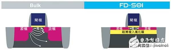
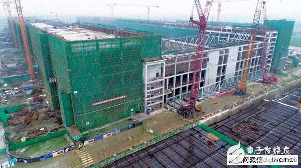
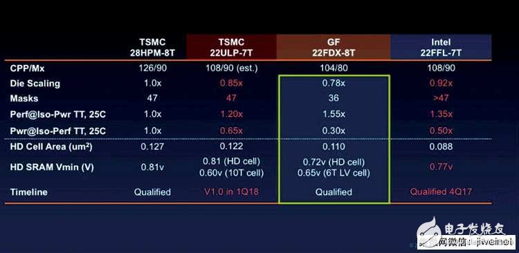
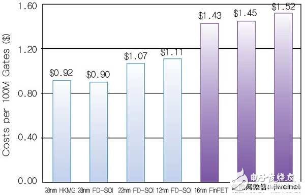
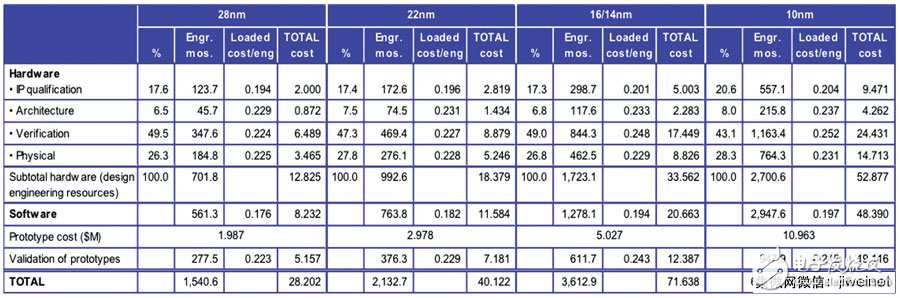
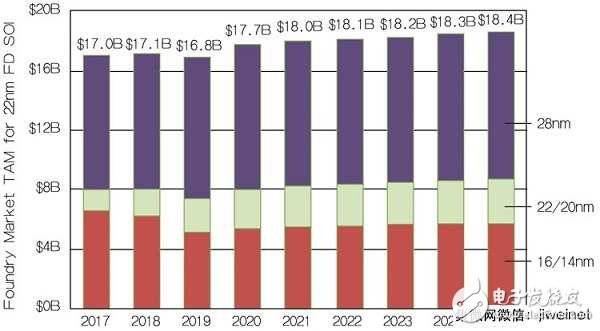
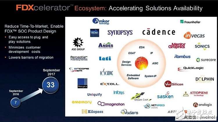
To say 2018 and the most notable semiconductor process technology in the next five years, in addition to the 7nm FinFET cutting-edge process to be mass-produced, and the 5nm process node that is expected to be fully integrated into extreme ultraviolet (EUV) lithography, each The foundry industry's focus on the wide-area, all-encompassing Internet of Things (IoT) market for low-power, low-cost component demand for a variety of low-end process technology options, is also the industry's focus. For example, foundry foundry TSMC 16 and 12 nm FFC (FinFET Compact Technology), 22 nm ultra low power (ULP), 28 nm HPC/HPC+, and 40 nm ULP, 55 nm Logic processes such as ULP and low power (LP), as well as Intel's 22nm low-power FinFET (22FFL) process, GlobalFoundries' 28nm HPP (High Performance Plus)/SLP (Super Low Power), The 22FDX process, as well as Samsung's 28nm FDSOI, LPP, LPH... and so on, are solutions for a wide range of IoT applications. Among them, the biggest difference between GlobalFoundries' FDX series process and Samsung's FD-SOI process, and other competing solutions, is the use of "full-vacuum insulation silicon-on-silicon" (English). Silicon On Insulator (FD-SOI) technology; this technology was first promoted in the industry by SOI Industry ConsorTIum, ST and its R&D partners IBM, GlobalFoundries, Samsung, etc. in 2011. The 28 nm and 20 (22) nanonodes can achieve comparable performance to the next-generation FinFET process supported by Intel, TSMC, etc., but at a lower cost and risk. Unlike the 3D transistor structure used in the FinFET process, FD-SOI is a planar process; according to the technical data on the ST official website, FD-SOI has two major innovations: first, the use of buried oxide (BOX) ultra-thin The insulating layer is placed on the silicon substrate; then the ultra-thin silicon film is deployed on the transistor channel. Because of its ultra-thin thickness, the channel does not need to be doped, so that the transistor can achieve complete depletion. The combination of the above two innovative technologies is called "ultra-thin body and buried oxide FD-SOI" (UTBB-FD-SOI). ST says that FD-SOI provides better transistor electrostatic characteristics than conventional bulk silicon technology, while buried oxide layers reduce the parasitic capacitance between the source and the drain; This technology effectively limits the flow of electrons between the source and the drain, significantly reducing the leakage current that affects component performance (Figure 1). In addition to passing through the gate, FD-SOI can also control transistor behavior by polarizing the underlying substrate of the component, similar to the body bias that can be achieved by bulk silicon technology. Figure 1: Comparison of bulk silicon process and FD-SOI process transistor structure However, the bulk bias of the bulk silicon technology is very limited because the parasitic leakage current and transistor geometry are reduced and the transistor efficiency is reduced. The FD-SOI has better bias efficiency due to the transistor structure and the ultra-thin insulating layer. In addition, the buried oxide layer can achieve higher substrate bias voltage, achieving breakthrough dynamic control of the transistor - when the polarization of the substrate is positive, that is, the forward substrate bias (FBB), the transistor switching speed can Speed ​​up and therefore optimize component performance and power consumption. According to ST, FD-SOI can easily implement FBB and dynamically adjust during transistor operation, providing design engineers with high flexibility, especially for components that are highly demanding in terms of power saving performance and speed, and performance is not critical. An ideal solution for portable/wearable consumer electronics applications. Market research firm InternaTIonal Business Strategies (IBS) CEO Handel Jones wrote in a report published in 2014: "The same 100mm square chip, the cost of using 28nm FD-SOI process is lower than the block CMOS process 3%, at 20 nm, it can be further down by 30%; this is because the higher the parameter yield, the lower the cost of the wafer;" In addition, the complexity of the FD-SOI process die and the bulk CMOS The process comparison is 10%~12% lower. Jones further stated: "With the combination of smaller die area and higher parameter yield, the product cost advantage of the FD-SOI process at the 20 nm node is 20% more than the bulk CMOS process; at the 28 nm node, The performance of FD-SOI is 15% higher than that of 20 nm bulk CMOS." He also pointed out: "The FD-SOI process can provide higher energy efficiency levels than the bulk CMOS process in high/low Vdd (energy efficiency). Levels); FD-SOI power efficiency in bit cells is also higher than bulk CMOS due to lower leakage current and better immunity to alpha particles." FD-SOI process: Western cold, oriental heat However, although FD-SOI claims to have many of the above advantages, the production yield of the process, the price of the dedicated wafer and the stability of the supply source, as well as the exact production time and overall technical support ecosystem integrity, the industry still has Many doubts; therefore, although FD-SOI has supporters such as ST and NXP in Europe, Samsung and GlobalFoundries have also actively promoted their own FD-SOI foundry business, which has been low in discussion and visibility in the market. Especially in the West. Time comes to February 2017, GlobalFoundries announced that it will invest 10 billion US dollars to establish a 12-inch wafer fab in Chengdu's high-tech western district in mainland China (Figure 2). The first production line that began operations in 2018 will be transferred from the company's Singapore plant. The more mature 180/130 nm process, the second phase is the 22FDX FD-SOI process line transferred from its Dresden plant in Germany , which is expected to start operations in 2019; this news has caused widespread repercussions in the semiconductor industry. In addition to demonstrating China's attempt to develop the local semiconductor industry chain, it also represents that the "main battle line" of the FD-SOI process will be ignited in China. Figure 2: Globalfoundries builds a 12-inch plant in Chengdu, China. Fab 11, the second-stage production line for mass production in 2019 is expected to be 22FDX FD-SOI process. China expressed its high interest in FD-SOI technology as early as 2015. At the time, Wayne Dai, CEO of China's IC design service provider VeriSilicon, said in an interview with EE TImes that it is constantly on the FinFET. In the process of chasing TSMC or Intel's footsteps, he believes that China should invest in FD-SOI and use this technology as an alternative to low-power processes. In addition, Shanghai Xingui Technology (Simgui) began mass production of the first batch of 8å‹ SOI wafers in the fall of 2015, using Smart Cut process technology with the company's strategic partner, French company Soitec. There is also an investment platform established by China's “big fundâ€. NaTIonal Silicon Industry Group (NSIG) announced in 2016 that it will acquire 14.5% of Soitec's equity; wafer foundry Shanghai Huali Microelectronics ( Shanghai Huali Microelectronics Corp.) revealed plans to invest in the FD-SOI production line before GlobalFoundries announced its Chengdu plant investment plan, but there is no specific timetable. These signs are showing that FD-SOI will be part of the blueprint for the development of China's semiconductor industry, and may make this technology, which has so far been so cold in the Western world market, shine in the eastern market. According to Alain Mutricy, senior vice president of product management at Globalfoundries, in an interview with EE Times in May 2017, the company's investment in Chengdu is only the first step. Next, the FD-SOI ecosystem will be established in the local area to help China. Fab IC design operators and design service providers are more likely to get the IP and tools they need. At the end of September 2017, at the 5th Shanghai FD-SOI Forum hosted by the SOI Industry Alliance , GlobalFoundries CEO Sanjay Jha once again publicized the FD-SOI process and used 22nm – a single mask. The smallest node is also suitable for cost/power sensitive applications such as IoT and portable devices. It is expected to be the "longevity" node in the market--based on the company's 22FDX process and Intel 22FFL process, TSMC 22ULP process. Performance comparison (Figure 3). Figure 3: Comparison of 22nm process performance between GlobalFoundries, TSMC and Intel Jha said in an interview with EE Times China after the special speech: "From the perspective of cost, if the 22nm FinFET adopts planar technology, the process steps will be more, and the process control complexity is very high. For FDX, the underlying substrate cost It may be a bit higher. It is really difficult to simulate the structure of the respective costs, but considering the construction investment in China and the cost effect of scale, the cost of production may be slightly higher than the technology of Intel. Advantage. " In the same forum, IBS CEO Jones also further proposed the cost per gate analysis of the FD-SOI process (Figure 4). He pointed out that the 28 nm FD-SOI process and 28 nm high dielectric cost gate metal gates (the HKMG) considerable bulk CMOS, the 22 nm gate FD-SOI costs to remain competitive; and to the next generation 12 nm FD-SOI, since the required mask layer The number is small, the gate cost is 22.4% lower than the 16nm FinFET process, 23.4% lower than the 10nm FinFET, and 27% lower than the 7nm FinFET, and the low power consumption of the FD-SOI is of course better than the FinFET. . Figure 4: Comparison of FD-SOI and FinFET Process Gate Costs Further Jones also raised cost hardware and software design of each process node comparison (FIG. 5), designed to estimate the cost of the FD-SOI 12 nm between 5,000 to $ 55 million, and 16 nm FinFET design cost of $ 72 million Around, the 10 nm FinFET design cost is about $131 million; because the design revenue is 10 times the cost, the potential market size (TAM) of the 12 nm FD-SOI will be 16 nm and 10 nm. The FinFET is larger. Figure 5: Comparison of design costs for each process node Combining FD-SOI's low power consumption and easy integration of RF features and cost advantages, GlobalFoundries sees mobile devices, IoT, wireless communications (5G/LTE/Wi-Fi), and automotive (ADAS/vehicle communications) as The popular application of the process; Jones believes that 90% of the existing 28nm process components are suitable for the FD-SOI process, and its TAM size is estimated to reach $17.1 billion in 2018 (Figure 6), even by 2025. With a total of 18.4 billion U.S. dollars, the FD-SOI technology suppliers can actually obtain a lot of revenue from each other, and the process of locking up the business opportunities in the IoT market has already started. Figure 6: Forecast of potential market size for 22 nm FD-SOI process Chinese IC manufacturers are eager to try, Taiwanese manufacturers? According to statistics provided by GlobalFoundries at the 5th Shanghai FD-SOI Forum, the company's 22FDX process has been favored by a total of 135 customers, 20 of which will enter multi-project wafer (MPW) trials by the end of 2017. Of the production, 15 of them will officially vote at the end of 2018, and these customers entering the test design/projection stage include 10 manufacturers from China. GlobalFoundries announced in February 2017 that it will build a 12-inch new plant with an investment of US$10 billion in Chengdu. In May of the same year, it announced with the Chengdu government that the two sides will cooperate to establish a cumulative investment of more than 100 million yuan in six years. The US dollar's "World-class FD-SOI Ecosystem" covers a number of research and development centers in Chengdu and research projects with universities and colleges to attract more top semiconductor companies to settle in Chengdu and to make Chengdu the next generation. Center of Excellence in Chip Design." Companies that will join the Chengdu FD-SOI ecosystem include EDA suppliers Cadence, Synopsys, design services provider VeriSilicon, Invecas, and chip design companies MediaTek, RockChip, and Shanghai Fudan Microelectronics (Shanghai) Fudan Microelectronics Group Company, etc.; Wei Weimin of VeriSilicon said in an interview with EE Times that he would receive R&D funding from the Chengdu FD-SOI ecosystem investment. "Every company must deploy a research and development team in Chengdu." Dai Weimin pointed out that the supporters of FD-SOI have already laid a solid foundation in China. Through activities such as the Shanghai FD-SOI Forum, they continue to publicize to local Chinese chip makers, IC design engineers, government officials, private investment funds, etc. And he believes that there are several important points to strengthen China's FD-SOI ecosystem, including: the feasibility of using FD-SOI to achieve mixed signal and RF design, the support of design service providers (such as core), and the implementation of substrate bias. Design processes and tools, as well as design teaching, seminars, university courses, labs and textbooks, and government support. Chinese IC industry is eager to try FD- SOI technology, and the local industrial ecosystem is gradually taking shape. Globally, GlobalFoundries said that its FD-SOI process ecosystem FDXcelerator partners have reached 33 in September 2017 (Figure 7). , covering the upstream and downstream industry of the semiconductor industry chain. Despite the small number of Taiwanese companies, including the packaging and testing giants ASE, embedded memory IP supplier Liwang Electronics (eMemory), and processor IP supplier Andes. Figure 7: GlobalFoundries actively builds an industrial ecosystem for the FD-SOI process Lin Zhiming, general manager of Jingxin Technology, said in an interview with EE Times that the company cooperated with Invercas, a long-term partner of GlobalFoundries and US IC design service provider, in 2015 to introduce its 32-bit N7 processor core into the reference design using FD-SOI process. Later, it also obtained the 22FDX process verification of GlobalFoundries. He noted that the processor core developed originally Crystal Heart of low power consumption, high efficiency demands of its N7, N8 and N9 series have been obtained using the networking and portable consumer electronics market, including smart stationed Watches, smart voice assistants, game consoles, and portable karaoke microphones, etc., the target market is in line with the direction of FD-SOI technology. With this process option and Crystal's IP, it is expected to bring better provinces to customers' designs. Electrical performance. Figure 8: Lin Zhiming, General Manager of Jingxin Technology: The terminal target market of the FD-SOI process is exactly the same as our product line. Taiwan's semiconductor IP suppliers are not absent from the FD-SOI ecosystem, but will Taiwan IC design operators follow up? In addition to MediaTek, which is already preparing to join the Chengdu FD-SOI ecosystem, local Taiwanese attitudes toward this technology are as cold as those in the Western market; such as the semiconductor testing laboratory iTech, it is understood that FD-SOI design is being tried. Taiwan's IC industry is still in a minority, and it is expected that the acceptance of the process will be much slower than that of mainland China. Huang Zhiyu, an analyst at the Semiconductor Research Center of Tektronix Industrial Research Institute, a market research organization in Taiwan, said that the current global FD-SOI capacity statistics are not easy to obtain, and only a rough estimate of the process will occupy the global wafer generation in 2017. The proportion of sales in the industry is about 0.2%; he also pointed out that mainland China is actively establishing the FD-SOI industry chain, introducing wafer manufacturer Soitec, wafer foundry GlobalFoundries, and 28nm process for Taiwan wafer foundry. Competitiveness can have an impact. However, Huang Zhiyu also pointed out that it is also important to observe the timing of China's FD-SOI capacity. It is necessary to consider both the depreciation of the 28nm process and the actual capacity of FD-SOI in the market. When the FD-SOI process capacity is small and the cost is relatively high, if the wafer foundry depreciates well, it will provide a more favorable 28nm process price, so in the cost-oriented terminal product competition, FD -SOI may not be beneficial." The 28-nm process can be said to be Taiwan's foundry duo UMC (UMC) and TSMC's "cash cow". Among them, TSMC's 28-nm wafer shipments in 2017 set a record high of 180,000. In the third quarter of 2017, TSMC’s revenue still accounted for the highest proportion of total revenue in the quarter, reaching 27%, higher than the advanced 16/20 nm node; UMC saw the market of 28 nm HKMG in the third quarter. Demand is slowing down. What impact will the FD-SOI process will have on the existing 28nm wafer foundry market? Will China's semiconductor industry rewrite history due to the development of FD-SOI technology? Will Taiwan Semiconductor Manufacturing Co., Ltd.'s 22nm new process be able to gain market momentum? For the Internet of Things market opportunity, what new "weapons" will UMC offer after the 28-nm process? The development of the semiconductor market in 2018 is worth watching! Dc Axial Fan ,12V Axial Fan,Dc Axial Fan 12V,Dc Axial Fan 24V Hangzhou Jinjiu Electric Appliance Co Ltd. , https://www.jinjiufanmotor.com