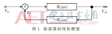
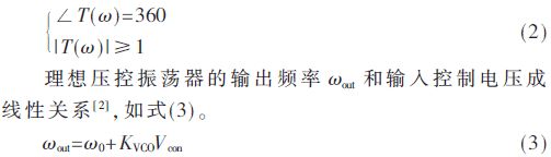
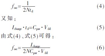
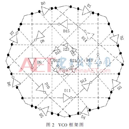
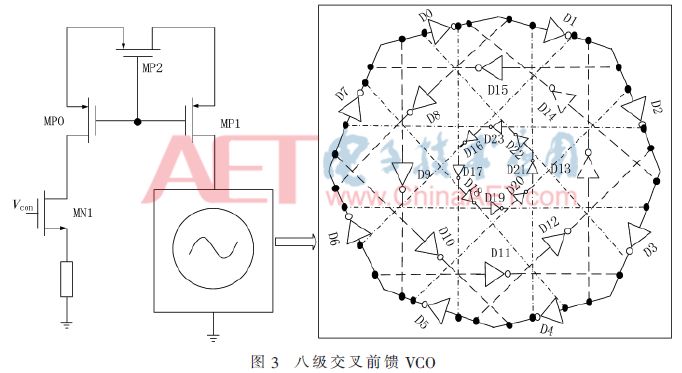
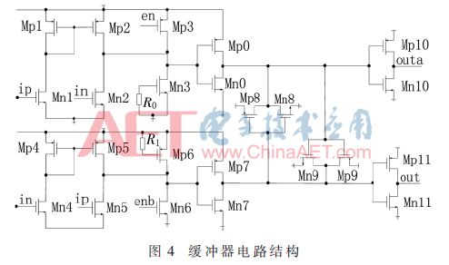
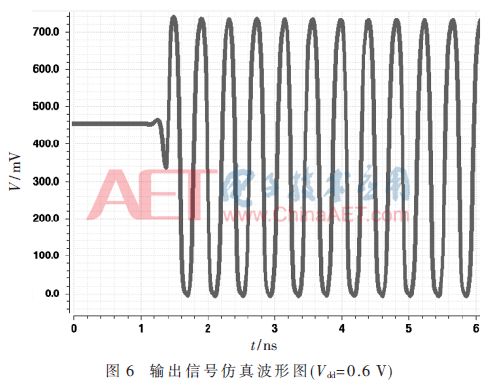
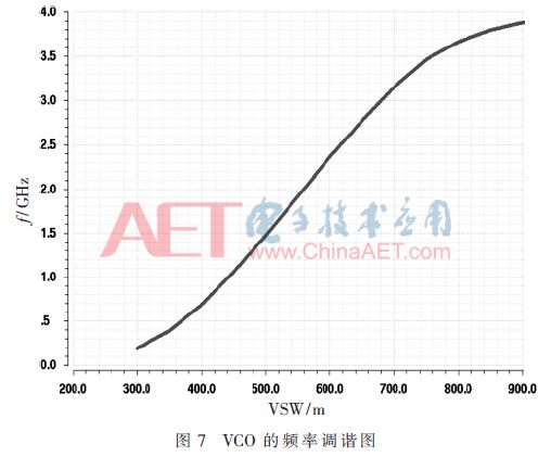
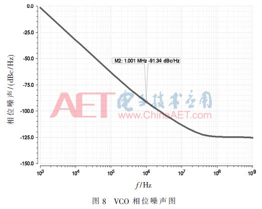
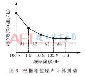
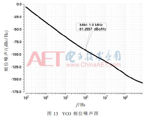
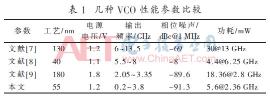
Aiming at the problems of high power consumption, large noise, and poor linearity of the ring oscillator, a novel cross feedforward ring oscillator circuit based on TSMC 55 nm technology is proposed. In-depth analysis of the device's own thermal noise, flicker noise contribution to the ring oscillator output phase noise percentage, the use of capacitive filtering technology to reduce the oscillator output phase noise, the use of the source negative feedback circuit to obtain a linear current to improve FM linearity, and provide Wide tuning range. Spectre RF simulation results show that the designed ring oscillator has a frequency coverage of 0.2 GHz to 3.8 GHz, 8 phases, phase noise of -91.34 dBc/Hz @ 1 MHz, and current consumption of 4.6 mA at 1.2 V supply voltage. Good degree. 0 Preface Voltage controlled oscillator (VCO) is an oscillator controlled by voltage to output frequency. It is an important module in wireless communication system and the core of phase locked loop (PLL). Its phase noise, sensitivity and other parameters directly affect The final performance of the PLL. The ring oscillator has a number of significant advantages over the LC-LCC: no inductor components are needed, saving chip area, cost savings, wide tuning range, and easy multi-phase implementation. However, the ring oscillator's phase noise performance is usually somewhat inferior. Considering its advantages of low power consumption, small area and high integration, ring oscillators are widely used in the field of communications. At present, the low-power, low-noise, wide-tuning new ring oscillator structure has attracted many scholars to invest in research. For example, in [1], a ring oscillator with a frequency range of 2.05 GHz to 3.35 GHz is designed, and its phase noise is For the -89.6 dBc/Hz@1 MHz, the power consumption of the core circuit is 18.36 mW, but its power consumption is large and cannot meet the low power consumption requirement in the wireless communication system. For the problems of large power consumption, large noise, and poor linearity of the oscillator, a novel ring oscillator structure is proposed. The ring oscillator has a frequency range of 0.2 GHz to 3.8 GHz, generates 8 phases, and the phase noise is − 91.34 dBc/Hz@1 MHz. 1 ring oscillator 1.1 Ring oscillator The core structure of the ring oscillator is a loop with positive feedback at an oscillation frequency, as shown in Figure 1. In the figure, HA(ω) is the transfer function of the basic amplifier and HF(ω) is the transfer function of the feedback network. The closed-loop gain of the feedback system is Equation (1): The operating principle of the ring oscillator is that the loop transfer function satisfies the Barkhausen criterion only at one frequency point, that is, it can oscillate if the formula (2) is satisfied at a certain frequency ω. Among them, ω0 represents the output frequency of the input voltage is 0, KVCO is the gain of VCO, the unit is rad/(s·V), Vcon is the control voltage. 1.2 Circuit Principle Analysis and Design The phase noise of the ring oscillator mainly comes from shot noise, thermal noise and environmental noise. Thermal noise is the result of temperature, bandwidth, and resistance; shot noise is caused by a dc bias current; and ambient noise is mainly due to the noise of the external power supply of the VCO and the noise of the substrate. The delay unit can adopt a single-ended structure and a differential structure. A differential ring oscillator composed of a differential structure as a basic delay unit has a good symmetry, and has great advantages in overcoming environmental noise, but not only increases due to a complicated circuit. The area of ​​the chip, but also bring more thermal noise, so the choice of a simple structure, a device with a single-ended structure, can effectively reduce the thermal noise caused by the device itself. An N-stage ring oscillator, with a delay of td per stage, the frequency of which is: Among them, Icharge is the charging current, Cpar is the total parasitic capacitance of the output node of the delay unit, and Vdd is the supply voltage. Taking into account the chip area, the design of the ring-shaped voltage-controlled oscillation is mainly composed of 24 inverters, as shown in Figure 2, which D0 ~ D8 are connected end to end to form a main ring structure. The input is represented by Vcon, and the VCO's oscillation frequency changes with the input voltage. As can be seen from Figure 3, the VCO mainly consists of three types of loops. The first type is the slowest main loop consisting of D0 to D8 eight delay elements, and the second type is a closed loop consisting of two four-level reverse delay elements. The loops, which are D9-D11-D13-D15 and D8-D10-D12-D14, respectively, also include four closed-loop loops, which are D16-D20, D17-D21, D18-D22, and D23-D19, respectively. The loop consists of a perfectly symmetrical relationship between the main loop and each sub-ring. By changing the current of the MN1 to change the negative resistance, the equivalent resistance of the drains of the MP0 and MP1 will also change, and the oscillation frequency will be adjusted. Because the power supply is low, MP0 and MP1 adopt a current mirror structure. The change of MP0, MP1 drain equivalent resistance will result in different output swings of different frequency signals, which will affect the noise performance of VCO. To meet the needs of communication systems, it is necessary to adjust the length ratio of the current mirror to optimize the voltage-controlled oscillator. Phase noise. According to the oscillation principle of the ring oscillator, this VCO composed of an eight-stage inversion delay unit as the main ring chain VCO can realize the quadrature-phase frequency signal output, and can effectively suppress the environmental noise in the clock data recovery circuit. Has an important application [5]. 1.3 Buffer Design In order to make the ring oscillator have a good output match, the buffer stage shown in Figure 4 is introduced in the circuit. It is mainly composed of differential pairs, single-ended inverters and latches. The output of the differential pair is used as the input of the inverter. This ensures the symmetry of the circuit. This buffer stage can change the output waveform of the ring oscillator to a clock signal with a duty cycle of 50% and can increase the drive capability. 1.4 layout design Layout design is an important part of the integrated circuit process. The layout design will directly affect the function of the chip. The ring oscillator designed in this paper is based on the TSMC 55 nm technology and focuses on the analysis of VCO matching and noise reduction problems. The layout rules are based on the layout rules and the virtuoso Layout Editor is used to perform layout and routing. The DRC and LVS are verified. The design of the ring oscillator layout is shown in Figure 5, with a core layout area of ​​70 μm x 81 μm. 1 Simulation results 2.1 Pre-imitation results Transient simulations were performed using the Cadence Spectre RF simulation tool. The results are shown in Figure 6. As can be seen from the figure, when Vdd = 0.6 V, the ring oscillator has a start-up time of approximately 1.4 ns and an oscillation amplitude of approximately 0.74 V. This result shows that the oscillator has a good start-up condition and a relatively short start-up time. The frequency tuning diagram of the VCO is shown in Fig. 7. It can be seen from Fig. 7 that when the control voltage is varied from 0 to 0.9 V, the VCO frequency tuning range is 0.2 GHz to 3.8 GHz and the tuning curve is 0.4 to 0.8 V. Has a good linearity. Phase noise is an important parameter and performance indicator of a voltage controlled oscillator. The phase noise performance of the voltage-controlled oscillator is obtained through the co-simulation of PSS and PNOISE. The frequency deviation range is set from 1 kHz to 1 GHz. When the tuning voltage is 0.6 V and the output center frequency is 2.4 GHz, the overall circuit phase noise curve is shown in Figure 8. It can be seen that the phase noise is -91.34 dBc/Hz at a frequency deviation of 1 MHz. Jitter and phase noise are both parameters that measure the ring oscillator's noise performance. Jitter is the uncertainty of the zero-crossing time of the oscillator's oscillation signal in the time domain. Phase noise is used to measure the spectrum purity of the oscillator in the frequency domain. They are essentially the same, but use different expression methods to describe the same phenomenon [6]. Calculating jitter from phase noise is shown in Figure 9. Let A = area = integrated phase noise power (dBc), then: The phase noise corresponding to each frequency offset in FIG. 9 is read in the phase noise graph shown in FIG. Calculated: Because the low-frequency VCO usually has large jitter, the PLL loop is generally used to effectively filter low-frequency noise. 2.2 Post simulation results After the revision and optimization of the layout, DRC and LVS verification, using the layout parameter extraction tool PEX on the layout of the parasitic resistance, parasitic capacitance and other parameters extracted. Figure 10 shows the schematic of the post-emulation circuit. After the layout parasitic parameters were extracted, the same simulation environment was set up, and simulation software was used to simulate the transient output signal waveform, frequency modulation characteristics and phase noise performance of the VCO during stable oscillation. The results of the post simulation were shown in Fig. 11 to Fig. 13 respectively. Show. From the figure, it can be seen that the post-imitation result is basically the same as the pre-imitation result. It can be seen that the layout design satisfies the frequency adjustment range of the oscillator between 0.2 GHz and 3.8 GHz, and the phase noise at the center frequency is -91.34 dBc/Hz@1 MHz. The consumption is 4.6 mW and the linearity is good. Table 1 summarizes the performance parameters of the designed ring voltage-controlled oscillator and compares them with oscillators with similar process conditions. It can be seen that the designed ring oscillator has a higher frequency and lower phase noise at low power consumption. 3 Conclusion Based on the TSMC 55 nm process, a 2.4 GHz low-power ring oscillator was designed with a cross feedforward circuit structure. The maximum power consumption of the entire ring oscillator was 5.6 mW at a supply voltage of 1.2 V, and the phase noise was -91.34 dBc/. Hz, the VCO has the advantages of low power consumption, low phase noise, and wide adjustable range. It can be applied to circuits such as phase-locked loops, frequency generators, and clock recovery. Copper Tube Terminals Without Checking Hole Our company specializes in the production and sales of all kinds of terminals, copper terminals, nose wire ears, cold pressed terminals, copper joints, but also according to customer requirements for customization and production, our raw materials are produced and sold by ourselves, we have their own raw materials processing plant, high purity T2 copper, quality and quantity, come to me to order it! Copper Tube Terminals Without Checking Hole,Cable Lugs Insulating Crimp Terminal,Cable Connector Tinned Copper Ring Terminal,Tubular Cable Lugs Crimp Terminal Taixing Longyi Terminals Co.,Ltd. , https://www.longyicopperterminals.com