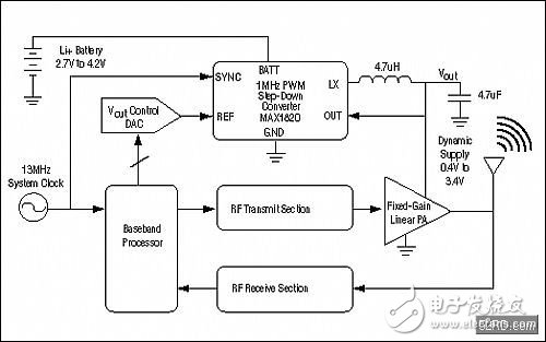
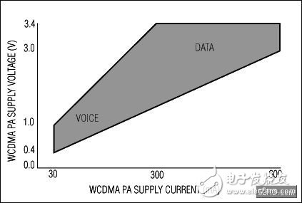
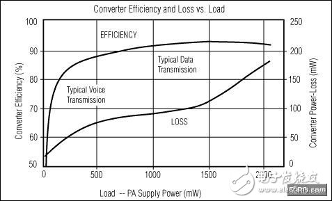
With the advent of the third generation of mobile communication (3G) era, mobile phone designers are busy developing new solutions to solve a series of new problems brought about by high-speed data transmission. Among them, the most important issues are in software, screen technology, data processing bandwidth and battery life. In second-generation (2G) phones that only have voice and low-speed data capabilities, the problem is not so severe, allowing for a simple and inexpensive solution to compromise. For example, a power amplifier (PA) used to transmit signals in a typical 2G handset is directly driven by the battery, albeit simple but not optimally efficient. In 3G mobile phones, high-speed data transmission requires higher bandwidth and transmission power, so in order to maintain long enough battery operating time, a more efficient solution must be adopted. Now, there is a solution that is increasingly popular among cell phone manufacturers, using a highly specialized step-down DC-DC switching regulator to drive the PA. The basic principle of the switching regulator to improve the transmission efficiency is to dynamically adjust the power supply voltage of the power amplifier so that it can meet the amplitude requirements of the RF signal in the power amplifier (see Figure 1). This regulation is implemented efficiently with a switching regulator, which saves battery power substantially under any operating conditions other than peak transmit power. Because the peak power is only needed when the mobile phone is far away from the base station and data transmission, in general, the power saving effect of this scheme is very significant. If the power supply voltage of the amplifier can be dynamically adjusted dynamically over a wide enough range, it is possible to use a linear amplifier with a fixed gain, eliminating the bias control (which has been widely used in current 2G phones). Of course, bias control can still be used to further increase control capabilities, and many cell phone manufacturers are actively tracking this approach; however, a company dominated by W-CDMA technology insists that bias control is not required. Figure 1. The switching regulator (MAX1820) dynamically regulates the power supply to the W-CDMA power amplifier (PA). Through the efficient adjustment of the power amplifier power supply, the energy consumption is greatly reduced, and the use time of the mobile phone battery is prolonged. Another issue that needs to be considered and related to system performance is what are the special performance requirements for this special purpose step-down switching regulator. In order to facilitate understanding, we should first study the load characteristics of the amplifier. Figure 2 is provided by a major cellular phone manufacturer to represent the load curve of a fixed-gain W-CDMA power amplifier in a bipolar process. At peak transmit power, the amplifier requires a 3.4V supply voltage and consumes 300mA to 600mA. At the lowest transmit power, that is, when the base station is close to the base station and only the voice is transmitted, the power amplifier draws only 30 mA of current, and the power supply voltage is 0.4V to 1V. The corresponding power consumption of the power amplifier is 2040mW (maximum value) and 12mW (minimum value). Figure 2. A typical resistive component of a fixed-gain bipolar W-CDMA power amplifier has a distinct resistive component. The power supply voltage and current will vary from the lowest 0.4V/30mA (12mW) to the highest 3.4V/600mA (2040mW). The voice transmission is generally performed at 1.5V/150mA (225mW), and the high-speed data is generally transmitted at 2.5V. Perform at /400mA (1000mW). Optimizing the switching regulator for such a power amplifier as a load is not an easy task. Maxim's MAX1820 W-CDMA cellular phone step-down regulator meets this requirement. The special features that distinguish the MAX1820 from other types of switching regulators are listed below: High efficiency over a wide range of loads—no high efficiency—switching regulators lose their meaning, so high efficiency and power savings are the dominant design considerations of the MAX1820 (see Figure 3). The low on-resistance (0.15Ω) PFET power switch inside the MAX1820 provides up to 93% efficiency when transferring data (approximately 500mW to 2040mW). When transmitting voice (approximately 12mW to 500mW), the MAX1820's internal 0.2Ω NFET synchronous rectifier and 3.3mA low operating current (forced PWM mode) achieve a conversion efficiency of 85%. The 85% efficiency doesn't sound too high, but it's not easy for a converter operating at 1MHz constant switching frequency and very light load. As shown in Figure 3, the converter has very low power loss. This is due to the excellent design and adoption of a sub-micron process that achieves lower gate capacitance for a given FET on-resistance. Dynamic adjustment of the output voltage - the output voltage needs to be adjusted between 3.4V and 0.4V. To do this, a digital-to-analog converter (DAC) is used to drive the analog control pin (REF) of the MAX1820. Since the output voltage range of the DAC is less than 3.4V, the converter has a voltage gain of 1.76 times from REF to OUT. Fast (30μsec) Output Slew Rate and Setup—In a W-CDMA system architecture, the transmit power needs to be adjusted 1dB up or down every 666μsec depending on the requirements of the base station. In addition, every 10ms, the mobile phone will enter or exit the data transmission mode, and accordingly a large transmission power jump will occur. In each case, the change in transmit power level needs to be completed in 50 μsec. However, considering the base station, DAC, and various system delays, the time left for the switching regulator to change the power of the power amplifier is reduced. For this reason, the MAX1820 is specifically designed to change and establish an output voltage within 30μsec, even for full-scale voltage and current changes. The MAX1820's output capacitance is limited to just 4.7μF due to the requirement for a fast change in output, which poses a challenge to the stability of the operation. The added benefit of a 4.7μF capacitor is that it allows a low ESR ceramic capacitor, which reduces the output ripple to 5mVpp. Another problem faced by buck regulators arises when it is necessary to quickly reduce the transmit power, such as when exiting data mode. In this case, the MAX1820 is able to reverse the current in the inductor and pull the output voltage down quickly to ensure a settling time of 30μsec. Otherwise, the linearity of the amplifier changes as the supply voltage drops slowly. In addition, this technology also saves power by returning the remaining power from the output capacitor to the battery at the input of the MAX1820. Stable operation from 9.5% to 100% PWM duty cycle and low dropout voltage—assuming the handset is powered by a single-cell Li-Ion battery, the input switching regulator has a voltage range of approximately 4.2V to 2.7V. In order to obtain a predictable noise spectrum and low output ripple, a constant switching frequency should be used. The MAX1820's forced PWM mode works stably until the battery is fully charged to 4.2V and requires a power supply voltage of 0.4V. 9.5% duty cycle. For its part, this is not difficult, but it should also take into account the opposite extremes. When a battery that has been discharged to a certain extent operates in a high-power data transmission mode, the duty cycle can be fully achieved at 100% and has a low dropout voltage. . To achieve a very low dropout voltage, the MAX1820's internal PFET is slightly over-designed to a very low 0.15Ω on-resistance. Assuming that the inductor has a series resistance of 0.1 Ω, the total voltage drop at a load of 600 mA is only 150 mV, which can be reduced year-on-year when the load is reduced. According to the requirements of the cellular phone manufacturer, when the battery is discharged to below 3.4V, a certain degree of reduction in the data transmission distance is acceptable. Breaking through this limitation requires a slightly more expensive and less efficient step-up/step-down regulator, which may require another full length discussion. 1MHz Switching Frequency and Synchronization—The MAX1820 has a 1MHz oscillator inside to control the PWM switching frequency. In the product definition phase of the MAX1820, increasing the switching frequency is one way to reduce the size of external components, but efficiency can be reduced to unacceptable levels. As mentioned earlier, the known noise spectrum and lower output ripple can be obtained using a fixed frequency PWM approach. The MAX1820's 1MHz internal clock has high accuracy and guarantees ±20% tolerance. In addition, for more accurate synchronization to the system clock, the MAX1820 includes a 13-way clock synthesizer that can feed a 10MHz to 16MHz Low amplitude sine wave. Figure 3. The MAX1820 step-down switching regulator is optimized for maximum efficiency when transmitting data with maximum battery drain. The 1MHz fixed switching frequency reduces output ripple and noise while maintaining relatively high efficiency and low power consumption when transmitting voice. The MAX1820 is currently used in 3G handset designs due to its unique performance. With the proven power-saving effect of the switching buck regulator in the W-CDMA power amplifier drive, this solution can also be used for other 3G standards and more different terminal devices, enabling miniaturized, personalized data phones and The ideal of wireless mobile computing becomes a reality.
The material of this product is PC+ABS. All condition of our product is 100% brand new. OEM and ODM are avaliable of our products for your need. We also can produce the goods according to your specific requirement.
Our products built with input/output overvoltage protection, input/output overcurrent protection, over temperature protection, over power protection and short circuit protection. You can send more details of this product, so that we can offer best service to you!
Lcd Adapter,Mini Size Lcd Adapter,Security Lcd Adapter,Waterproof Lcd Adapter Shenzhen Waweis Technology Co., Ltd. , https://www.laptopsasdapter.com