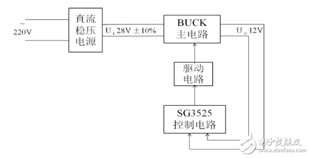
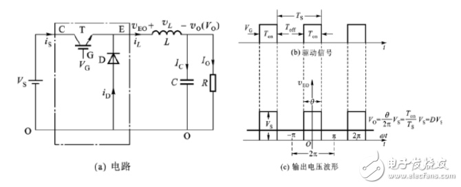
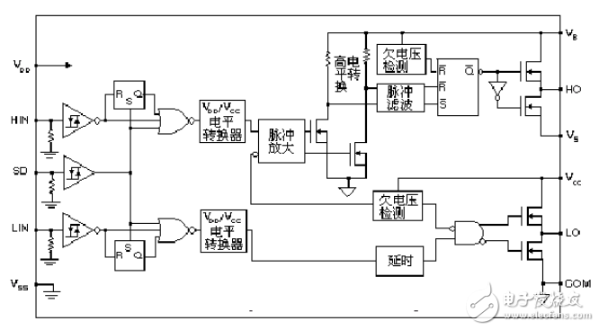
This article brings you to the introduction of buck converter design. This design is mainly for the main circuit of the BUCK converter, and the selected full-control device is P-MOSFET. For related information, a PWM control signal can be generated by using a control circuit based on a pulse width modulator SG3525 chip to control the on and off of the P-MOSFET. Then, by designing the driving circuit of the IR2110 as the main chip to drive the P-MOSFET, the circuit needs to use two power supplies with a constant output voltage of 15V to drive the two chips to work. At the same time, the voltage closed loop is used, and the output voltage is divided and processed, and then fed back to the control end. The PWM signal is generated by comparing the output voltage with the carrier signal to achieve the purpose of negative feedback stability control, and the circuit block diagram 1 is obtained. Figure 1 general circuit block diagram Figure 2 below shows the basic structure of a BUCK type DC/DC converter. This circuit is mainly composed of a full-control switch tube T and a freewheeling diode D and an output filter circuit LC in a dashed box. By periodically turning on and off the switching tube T, the input voltage Vs of the DC power source can be converted into a voltage Vo and output to the load. Figure 2 Circuit structure of the Buck converter Considering that IR2110 has both optocoupler isolation and electromagnetic isolation, and the circuit chip is small in size, high in integration, fast in response, strong in driving capability, undervoltage lockout, low cost, easy to debug, and external protection blockade. The advantages of the port, etc., in this design, the IR2110 is used as the main driver chip. The IR2110's internal functions consist of three parts: logic input; level shifting and output protection. The characteristics of the IR2110 as described above can bring a lot of convenience to the design of the device. In particular, the design of the high-end floating bootstrap power supply can greatly reduce the number of driving power supplies, that is, a set of power supplies can control the upper and lower ends. Its internal circuit diagram is shown in Figure 3. Figure 3 IR2110 internal circuit Although the main advantage of the IR2110 is that a set of power supplies can achieve control of the upper and lower ends, unfortunately, only one switch tube is used in the design of the BUCK converter circuit, so the advantages of the IR2110 are not fully reflected. Considering the design convenience, select 12 pins as the input terminal, 1 pin as the output terminal, and 2 pin to the S pole of the P-MOSFET switch tube, so that the IR2110 can drive the switch tube normally. flyphotography SHAOXING SHANGYU FEIXIANG PHOTOGRAPHIC CO.,LTD , https://www.flying-photography.com