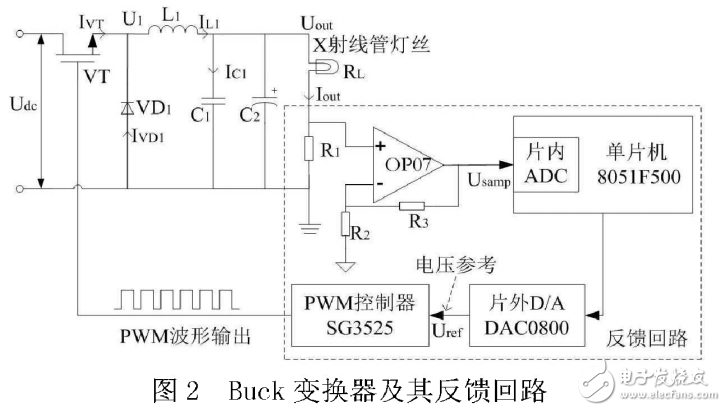
Radiation logging is an important part of the logging method. Compared with r-rays, X-rays have the advantages of easy access, radiation control, environmental protection, etc. The filaments of X-ray tubes are widely used for heating by high current (0~2A). A large number of free electrons are generated, and the free electrons are accelerated by the strong electric field of the high-voltage power source. The accelerated high-speed free electrons bombard the anode target, and the filament supply current of the X-ray X-ray tube can adjust the intensity of the radiation. If the voltage source is used for power supply, Since the filament resistance will increase with the increase of the energization time, the filament resistance is not a constant value, and the fluctuation of the filament resistance will cause the current to fluctuate, thereby affecting the stability of the radiation intensity emitted by the X-ray machine. The X-ray has strong radiation. Ability, long-term exposure is very harmful to human tissue, so it should avoid the operator's close-range operation based on the above problems. This paper designs and develops a hardware circuit. The hardware system is shown in Figure 1. The whole system consists of single-chip microcomputer, button, liquid crystal display, D/A converter, A/D converter, 485 communication interface and constant current circuit formed by switching power supply. The single-chip microcomputer of this system is processed by SiliconLab. Chip C8051F500, the chip is an 8-bit 51 core structure, the main frequency can reach 50MHz, the chip integrates 12-bit successive comparison type A/D converter, the highest sampling rate can reach 200KPS, and the on-chip automatic reference voltage is external 48 A pin, a UART, a general SPI, a CAN bus and other rich communication interfaces. On-chip integration of up to 64KFLASHROM space, can store more complex code, and has 4KXRAM, no need to externally expand RAM. Buck converter is also called buck converter. The structure is shown in Figure 2. Udo is a stable DC power supply, VT is a switching transistor, VD1 is a freewheeling diode, L1 is a storage inductor, and capacitors C1 and C2 are used to filter ripple. The energy storage feedback loop is composed of a current sampling resistor R1, an operational amplifier OP07, an on-chip A/D converter and a DAC0800. The single-chip microcomputer is the control core, and the D/A converter supplies the reference voltage Ur for the PWM controller. When the switch tube VT is turned on, the voltage U. Equal to the input voltage Uout, diode VD. In the reverse cut-off state, current IVD, zero current IVT=ILI, flowing through the inductor L1, the current increases linearly. When the PWM wave level changes, the switch is turned off, the inductance L. In order to keep its current IL1 from mutating, the inductance L. The magnetic field in the medium will change the polarity of the voltage across it. At this time, the diode VD1 is forward biased and has a current IVD flowing through the diode VD. The current IL1 across the inductor L is kept continuously changing, so VD1 is a freewheeling diode at the time ILl "lout, the capacitors Cl, C2 are in discharge: l dog state; when ILl" lout capacitors Cl, C2 are in charge state capacitors Cl, C2 are favorable The output current Iout, and the output voltage Uout are kept constant. The switching frequency of the switching power supply depends on the oscillation frequency of the PWM controller Sg3525 at the output end, the output current Iout flows through the resistor R1, and a voltage drop occurs across R1, and the voltage across the resistor R1 is performed. Sampling, amplified by the operational amplifier and sent to the internal A/D of the microcontroller, according to the theory of operational amplifiers: Usamp=RlIout(l+R3/R2) According to the above formula: Iout=Usamp/(R1+RIR3/R2) Using the C8051F500 internal A/D converter, the sampled data reflects the current value of the power supply output. The sampling interrupt is started every sampling end. The sampling current IOLit is calculated by the interrupt function, and the preset current value Iset and the sampled current value are obtained. I compare, adjust the reference voltage Uref according to the error size, pass the reference voltage to the PWM controller Sg3525 via the D/A converter DAC0800, and then change the duty cycle of the PWM wave to adjust the on-time of the switching transistor VT, and adjust the output. The relationship between the voltage U, U and the duty ratio D is as follows: Um=DUdo 1.00Mm Wafer Connector,1.0Mm Single Row Smt Wafer Connector,1.0Mm Smt Wafer Connector,1.0Mm Dual Row Smt Wafer Connector Shenzhen CGE Electronic Co.,Ltd , https://www.cgeconnector.com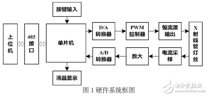
introduction