In a switching circuit, each PIN diode has an accompanying PIN diode driver or switch driver that provides controlled forward bias current, reverse bias voltage, and control signals (usually a digital logic command) with one or more Active interface between PIN diodes. Depending on the application, this drive function can be implemented in a discrete design or specialized IC. PIN diode Figure 1 PIN diode Figure 2 PIN diode equivalent circuit: a) conduction, IBIAS >> 0; b) cutoff, VBIAS ≤ 0 Figure 3 Silicon diode on-resistance and forward current Figure 4 Relationship between silicon diode capacitance and reverse voltage The PIN diode bias interface connects the switch driver control circuit to the PIN diode to switch the diode by applying a forward or reverse bias, which is a challenging task. The bias circuit typically uses a low pass filter between the RF circuit and the switch driver. Figure 5 shows a single pole double throw (SPDT) RF switch and its bias circuit. When set, filters L1/C2 and L3/C4 allow control signals to be applied to PIN diodes D1–D4, and the interaction between the control signal and the RF signal (switching from RF IN to PORT 1 or PORT 2) is minimal. These components allow a relatively low frequency control signal to pass through the PIN diode, but prevent high frequency signals from escaping from the RF signal path. Abnormal RF energy loss means that the insertion loss of the switch is too high. Capacitors C1, C3, and C5 prevent the DC bias applied to the diode from invading the circuitry in the RF signal path. Inductor L2 in the DC ground loop allows DC and low frequency switch driver signals to pass easily, but exhibits high impedance for RF and microwave frequencies, reducing RF signal loss. Figure 5 Typical single pole double throw (SPDT) RF switch circuit Figure 6 discrete switch driver circuit The operational amplifier PIN diode driver op amp circuit is an attractive alternative to PIN diode driving. In addition to flexibility, such circuits often operate at transition speeds approaching or exceeding 1000V/μs. Three different RF PIN diode amplifier drive circuits are described below. The selected amplifiers, although different in fundamental characteristics, perform similar functions. These amplifier circuits can drive silicon or gallium arsenide (GaAs) PIN diodes, but each has its own characteristics. AD8037 - Clamping Amplifier This circuit operates at frequencies up to 10MHz with excellent switching performance and a total propagation delay of 15ns. By varying the gain or clamping voltage, the output voltage and current can be adjusted to suit different applications. The AD8037 clamp amplifier was originally designed to drive the ADC and provides a clamp output to protect the ADC input from overdriving. The configuration shown in Figure 7 drives the PIN diode with a pair of AD8037 (U2 and U3). Figure 7 AD8037 PIN Diode Driver Circuit The AD8137—differential amplifier differential amplifier (the AD8137 used in this example) provides excellent high-speed switching performance at low cost and gives designers the flexibility to drive all types of RF loads. A wide variety of differential amplifiers are available, including faster and higher performance devices. Figure 8 PIN diode driver schematic ADA4858-3—Three-Channel Operational Amplifier with Charge Pump Built-in Many applications only provide one power supply, which often makes circuit designers feel embarrassed, especially when low-off capacitance is required in the PIN circuit. In this case, the silicon or GaAs PIN diode driver circuit can use an on-chip integrated charge pump op amp without the need for an external negative supply; the benefit is significant space, power, and budget savings. Figure 9 GaAs CT capacitance versus voltage Figure 10 ADA4858-3 used as a PIN diode driver Figure 11 Functional block diagram of the downconverter Figure 12 shows the waveform of the RF switching speed Figure 13 Spectrum response of the downconverter Conclusion The above three examples show that the op amp can be used creatively as an alternative to conventional amplifiers, and its performance is comparable to that of PIN diode-specific driver ICs. In addition, the op amp provides gain adjustment and input control, and when using an op amp with a built-in charge pump, no negative supply is required, which increases the design flexibility of the PIN diode driver and other circuitry. Op amps are easy to use and configure, making it easy to solve complex problems. COB Light
COB LED par light for theatre, productions, TV studio, stage
Description:
COB200-2in1 is a professional theatre fixture that utilizes a 200W warm-white and cold-white COB LED with a color temperature of 3200k-6000K. Users are able to creat a customized color tempreature via a DMX Controller or set directly on the display menu. It offers a high-power light output with rich hues and smooth color mixing for stage and wall washing. The double bracket makes installing easily and versatile.
Our company have 13 years experience of LED Display and Stage Lights , our company mainly produce Indoor Rental LED Display, Outdoor Rental LED Display, Transparent LED Display,Indoor Fixed Indoor LED Display, Outdoor Fixed LED Display, Poster LED Display , Dance LED Display ... In additional, we also produce stage lights, such as beam lights Series, moving head lights Series, LED Par Light Series and son on...
COB Light Series,Led Par Light,54 Led Par Light,Par Led Lights Guangzhou Chengwen Photoelectric Technology co.,ltd , https://www.cwledpanel.com Below is the circuit diagram of [Drive PIN Diode Replacement Component Selection]
On the other hand, it is also possible to use an arbitrary operational amplifier and a special amplifier such as a clamp amplifier or a differential amplifier as an alternative to the discrete PIN diode drive circuit and the expensive PIN diode driver IC. These op amps have a wide bandwidth, high slew rate, and ample steady state current to drive the PIN diode. This article discusses three different PIN driver circuits that use op amps or special amplifiers: the AD8037, AD8137, and ADA4858-3. These circuits are designed for single-pole, double-throw (SPDT) PIN diode switches, but they can be modified to suit other circuit configurations. Before describing these circuits in detail, this article will first discuss the characteristics and use of PIN diodes.
The PIN diode is used as a current-controlled resistor that operates at RF and microwave frequencies. It has a resistance of only a fraction of an ohm when forward biased ("on") and up to 10kΩ when reverse biased ("off"). . Unlike a typical PN junction diode, a high-resistance intrinsic semiconductor material (indicated by the "I" in the PIN) is added between the P and N regions of the PIN diode, as shown in Figure 1. 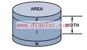
When the PIN diode is forward biased, holes from the P material and electrons from the N material are implanted into the I region. The charge does not complete recombination immediately; the finite amount of time required for charge recombination is called the "carrier lifetime." This results in a net stored charge in the I region, and thus its resistance drops to a value called the effective on-resistance RS of the diode (see Figure 2a). 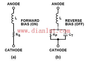
When a reverse or zero bias voltage is applied, the diode appears as a large resistor RP that is in parallel with the capacitor CT (see Figure 2b). By changing the diode geometry, PIN diodes can be combined with different RS and CT to meet the needs of various circuit applications and frequency ranges.
The steady state bias current ISS and the reverse voltage provided by the driver together determine the final values ​​of RS and CT. Figure 3 and Figure 4 show the relationship between the typical PIN diode series - M/A-COM MADP 042XX8-13060 series silicon diodes. Diode materials can affect their properties. For example, gallium arsenide (GaAs) diodes require little reverse bias to achieve low CT values, as shown in Figure 9. 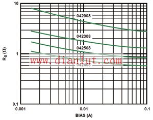

The charge stored in the PIN diode can be approximated using Equation 1.  (1)
(1)
Where QS is the stored charge; Ï„ is the diode carrier lifetime; ISS is the steady state current.
To turn the diode on or off, the stored charge must be injected or removed. The job of the drive is to inject or remove stored charge at an extremely fast rate. If the switching time is less than the carrier lifetime of the diode, Equation 2 can be used to approximate the peak current (IP) required to achieve fast switching. 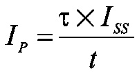 (2)
(2)
Where: t is the required switching time; ISS is the steady-state current provided by the driver to set the PIN diode on-resistance RS; Ï„ is the carrier lifetime.
The driver injects or removes current (or "spike current") i can be expressed as Equation 3. 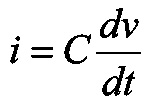 (3)
(3)
Where C is the value of the driver output capacitor (or "spike capacitance"); V is the voltage across the output capacitor; dv/dt is the time rate of change of the voltage across the capacitor. 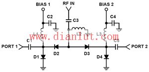
Bias circuits, RF circuits, and switch driver circuits all interact to affect each other's performance, so like all designs, it's important to consider the various factors. For example, larger C2 and C4 (>20pF) are good for RF performance, but are troublesome for drivers because large capacitances cause slower rising edges and falling edges. Fast switching is beneficial for most applications; therefore, in order to achieve optimal driver performance, the capacitance must be extremely small, but in order to meet RF circuit requirements, the capacitance must be large enough.
Traditional PIN diode driver
PIN diode drivers are available in a variety of shapes and sizes. Figure 6 shows a schematic of a typical discrete switch driver that provides high switching speed. This driver can be implemented either in a "slice" (hybrid) structure or in a "surface mount" (SMT) device; the former is very expensive, while the latter is inexpensive, but requires a printed circuit board (PCB) More area than mixed structure. 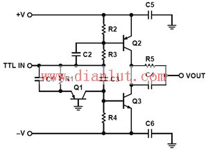
There are also dedicated switch driver integrated circuits (ICs). These ICs are very compact, offer a TTL interface, and have good performance, but they are limited in flexibility and often expensive.
There is also a switch driver architecture that should be considered, that is, an operational amplifier. The obvious advantage of an op amp switch driver is its flexibility, which can be easily configured to suit different applications, supply voltages and conditions, providing designers with a wealth of design options. 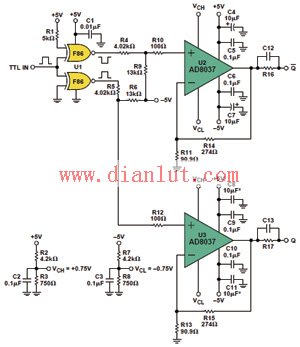
In this example, U2 and U3 are configured in phase with a gain of 4. Extremely clean and precise clamping is achieved with the unique input clamp feature of the AD8037. It linearly amplifies the input signal up to the gain multiplied by the positive and negative clamp voltages (VCH and VCL). When the gain is 4 and the clamp voltage is ±0.75V, if the input voltage is less than ±0.75 V, the output voltage is equal to 4 times the input voltage; if the input voltage is greater than ±0.75V, the output voltage is clamped at the maximum ±3V . This clamp feature allows overdrive recovery to be very fast (typically less than 2ns). The clamp voltages (VCH and VCL) are determined by voltage dividers R2, R3, R7 and R8.
The digital interface is implemented by the 74F86 XOR logic gate (U1), which provides the drive signals used by U2 and U3. The propagation delay skew between the two complementary outputs is minimal. Resistor networks R4, R5, R6, and R9 convert the TTL output level to approximately ±1.2V and then feed to U2 and U3 through R10 and R12.
The ±1.2-V inputs of U2 and U3 provide 60% overdrive to ensure that the output will enter the clamp state (4 x 0.75V). Therefore, the output level of the silicon PIN diode driver is set to ±3V. Resistors R16 and R17 limit the steady state current. Capacitors C12 and C13 set the peak current of the PIN diode.
The high speed differential amplifier AD8137 is typically used to drive an ADC, but can also be used as a low cost, low power PIN diode driver. Typical switching times are 7 to 11 ns, including the propagation delay of the driver and RF load. It offers complementary outputs and is versatile and can replace expensive traditional drives.
The circuit shown in Figure 8 converts a single-ended TTL input (0 to 3.5V) into a complementary ±3.5V signal while minimizing propagation delay. The TTL signal is amplified four times and produces the required ±3.5V swing at the output of the AD8137. The midpoint (or common mode voltage) of the TTL signal is 1.75V; the same voltage must be applied to R2 as the reference voltage, VREF, to avoid introducing common mode offset errors at the amplifier output. It is best to drive this point from a low source impedance; any series impedance will increase to R1, which affects the amplifier gain. 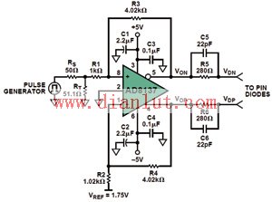
The output voltage gain can be calculated by Equation 4:  (4)
(4)
To properly terminate the input impedance of the pulse generator to 50Ω, the input impedance of the differential amplifier circuit needs to be determined. This can be calculated using Equation 5, resulting in RT = 51.55 Ω, the closest standard 1% resistance value is 51.1 Ω. For a symmetrical output swing, the impedance of the two input networks must be the same. This means that the inverting input impedance must incorporate the signal source's impedance and termination resistance into the gain setting resistor R2.  (5)
(5)
In Figure 8, R2 is approximately 20 Ω greater than R1 to compensate for the additional resistance (25 Ω) introduced by the parallel combination of source resistance RS and termination resistor RT. Set R4 to 1.02kΩ (the closest standard resistance value of 1.025kΩ) to ensure that the two resistor ratios are equal, avoiding the introduction of common mode errors.
Output level shifting is easily accomplished using the VOCM pin of the AD8137, which sets the DC output common-mode level. In this example, the VOCM pin is grounded to provide a symmetrical output swing with respect to ground.
Resistor R5 and R6 set the steady state PIN diode current as shown in Equation 6.  (6)
(6)
Capacitors C5 and C6 set a spike current that helps inject and remove the charge stored in the PIN diode. The values ​​of these capacitors can be adjusted to optimize performance based on specific diode load requirements. The peak current can be calculated by Equation 7.  (7)
(7)
The ADA4858-3, a high-speed current-feedback three-channel amplifier, is an excellent device with an on-chip charge pump that can swing from 3 to 1.8V below ground (depending on supply voltage and load). The device is robust enough to provide up to 50mA of negative supply current for other circuits.
The ADA4858-3 provides a unique solution for complementary PIN diode microwave switch drive problems in single-supply systems. Looking back at Figure 4, it can be seen that even a small amount of reverse bias helps to reduce the diode capacitance CT, depending on the type of PIN diode. Such drivers are advantageous for GaAs PIN diodes because they typically do not require a large negative bias to keep the shutdown capacitor (CT) small (see Figure 9). 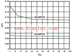
The circuit shown in Figure 10 uses the ADA4858-3 as the PIN diode driver. A buffer gate can be added to the input to make the circuit compatible with TTL or other logic. The requirement for this circuit is to convert the TTL 0V to 3.5V input signal swing to a complementary –1.5 to +3.5V swing for driving the PIN diode. 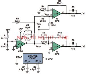
R1, R2, R3, and U1C form the -1.5V reference voltage for the circuit, and the internal negative voltage CPO is generated by the on-chip charge pump. Capacitors C3 and C4 are required for charge pump operation. The negative reference voltage is then passively combined with the VTTL input through a voltage divider (R5 and R9), and the resulting voltage (VRD) appears at the non-inverting input of U1B. The U1B output voltage can be calculated using Equation 8.  (8)
(8)
among them:  (9)
(9)
The negative reference voltage is also fed to amplifier U1A where it is combined with the TTL input and the resulting output voltage V2 can be calculated using Equation 10.  (10)
(10)
These amplifiers use a current feedback architecture, so care must be taken to select the feedback resistors that play an important role in the stability and frequency response of the amplifier. For this application, the feedback resistor is set to 294Ω, which is the value chosen in the data sheet. The output voltages V1 and V2 can be expressed by Equation 8 and Equation 10, respectively. The amount of output spike current can be determined using Equation 3 and the voltage across capacitors C5, C6. The steady-state current setting the PIN diode on-resistance is determined by the voltage difference across R11 and R12 and depends on the PIN diode curve and system requirements.
For this application, the RF switching load is the MASW210B-1 silicon PIN diode single-pole double-throw (SPDT) switch for the front end of the microwave downconverter (see Figure 11). 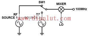
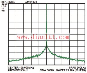
The switch output waveform and TTL input signal are shown in Figure 12. Please note that the rising and falling edges are very steep. Since the switching time requirement of the switch is relatively slow (approximately 50 ns), the peak capacitors C5 and C6 are not used in this application. The resistors R11 and R12 that set the steady-state diode current are both 330Ω. 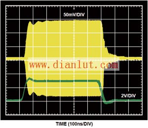
Figure 13 shows the spectral response of the front end of the downconverter; switch SW1 is in a fixed position to eliminate insertion loss. Note that there are no harmonics or sidebands in the figure, which fully indicates that no significant 100 kHz switching artifacts are dissipated from the ADA4858-3 on-chip charge pump, which is an important consideration in the use of these devices in such applications.