
According to the teacher's teachings many years ago, we usually put equal impedance on the two inputs of the op amp. Why is there such a rule of thumb? Should we follow this approach? Please think about 30 seconds first...
Let's take a look at the teacher's teaching...
If you grew up in the era of the 741 op amp, then the concept of balancing the input resistance of an op amp must be rooted in your mind. Over time, this may no longer be true due to the emergence of different circuit technologies and different IC processes. In fact, it can cause more DC errors and more noise, making the circuit more unstable. Why did we do that before? What changes have caused us to do so now may be wrong?
In the 1960s and 1970s, the first generation of operational amplifiers were fabricated using a common bipolar process. For reasonable speed, the differential pair tail current is typically in the range of 10 μA to 20 μA.
The beta value is 40 to 70, so the input bias current is around 1 μA. However, the transistor matching is not so high, so the input bias currents are not equal, resulting in a 10% to 20% deviation between the input bias currents (referred to as "input offset current").
Adding a resistor (R3 in Figure 1) equal to the parallel combination of input resistor R1 and feedback resistor R2 at the non-inverting ground input allows the impedance to be equal. It can be proved by some calculations that the error is reduced to Ioffset × Rfeedback. Since Ioffset is 10% to 20% of Ibias, this will help reduce output offset errors.
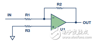
Figure 1. Classic Inverting Amplifier
From the three indicators, is the above teaching completely correct?
1. DC error
To reduce the input bias current of bipolar op amps, many op amp designs integrate input bias current cancellation. OP07 is an example. The increase in the input bias current cancellation function greatly reduces the bias current, but the input offset current may be 50% to 100% of the residual bias current, so the effect of increasing the resistance is very limited. However, in some cases, increasing the resistance may result in an increase in output error.
2. Noise
The resistance thermal noise is calculated as √4kTRB, so the 1 kΩ resistor will have 4 nV/√Hz noise. Increasing the resistance increases the noise. In Figure 2, surprisingly, although the 909 Ω compensation resistor is the lowest value resistor, it contributes the most noise to the output of Figure 2 due to the noise gain from this node to the output. The output noise caused by R1 is 40 nV/√Hz, R2 is 12.6 nV/√Hz, and R3 is 42 nV/√Hz. Therefore, do not use a resistor. On the other hand, if the op amp is powered by dual supplies and one power supply is powered up before the other, an ESD network may have a latch-up problem. In this case, it may be desirable to add a certain resistance to protect the device. However, if used, a bypass capacitor should be placed on the resistor to reduce the noise contribution of the resistor.
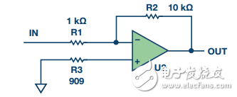
Figure 2. Noise analysis
3. Stability
All op amps have a certain input capacitance, including differential mode and common mode. If the op amp is connected as a follower and a resistor is placed in the feedback path to balance the impedance, the system may be susceptible to oscillation. The reason is that the large feedback resistor, the input capacitance of the op amp, and the stray capacitance on the PC board form an RC low-pass filter (LPF). This filter causes a phase shift and reduces the phase margin of the closed loop system. If it is reduced too much, the op amp will oscillate. One customer used the AD8628 CMOS operational amplifier in a 1 Hz Sallen-Key low-pass filter circuit. Due to the low corner frequency, the resistance and capacitance are quite large (see Figure 3).
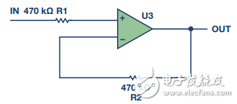
Figure 3. What you see
The input resistance is 470 kΩ, so the customer places a 470 kΩ resistor in the feedback path. This resistor together with an input capacitance of 8 pF (see Figure 4) provides a 42 kHz pole. The gain bandwidth product of the AD8628 is 2 MHz, so it still has a lot of gain at 42 kHz and rail-to-rail oscillation occurs. Replacing the 470 kΩ resistor with a 0 Ω jumper solves the problem. Therefore, large resistors should be avoided in the feedback path. Here, which is large depends on the gain bandwidth of the operational amplifier. For high-frequency op amps, such as the ADA4817-1 with a gain-bandwidth product over 400 MHz, the 1 kΩ feedback resistor is called a large resistor. Be sure to read the data sheet for advice.
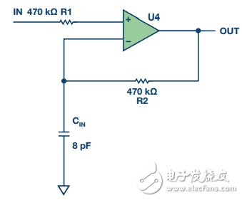
Figure 4. Seeing the electronics
Of course, years of practice will certainly produce some useful rules of thumb. However, when reviewing the design, it is best to review these rules of thumb to determine if they still apply. Regarding the need to increase the balancing resistor, if it is a CMOS, JFET or bipolar op amp with input bias current cancellation, it may not need to be increased.
Ningbo Autrends International Trade Co.,Ltd. , https://www.ecigarettevapepods.com