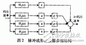
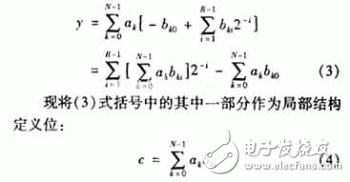
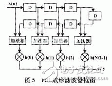
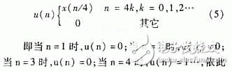
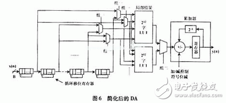
Many telecom companies today are closely watching the development and development of their 3G products, such as mobile terminals, base stations and other large network equipment. Undoubtedly, 3G products and services have become the mainstream of the wireless communication market, and CDMA, especially wideband CDMA (W-CDMA), relies on its high performance, high efficiency in system capacity utilization, and physical resource usage. Convenience is increasingly becoming the dominant in 3G technology. In order to meet the high technical complexity of 3G and high signal processing requirements, FPGA/ASIC-based dedicated hardware must meet the specifications of different user products. That is to say, in the development of 3G wireless terminals, the parameters of product size, weight and power consumption will be very important and important determinants. As a result, system-on-chip (SoC) has been introduced into the development of 3G as a new design strategy. SoC requires the ability to integrate regional effective signal processing algorithms and structure design and development on a small chip. As the most common component in signal processing, digital filters are widely used in various parts of wireless communication. This paper discusses the ASIC implementation of the pulse shaping FIR filter in 3G standard CDMA 2000, and proposes a practical implementation structure: a table lookup method based on distributed computing (DA) structure. Pulse shaping filters are commonly used in baseband communication transmissions designed to improve the efficiency of signal spectrum transmission. The D/A-converted shaping filter is usually designed as an FIR filter, which functions as [1]: converts the in-phase (I) and quadrature (Q) symbols of the signal into analog I and Q signals. In general, FIR filters need to have a raised cosine or a square root raised cosine shaped impulse response. It should be noted here that the sampling rate of the shaping filter is generally higher than the input I and Q symbol rate (usually 4 to 8 times). Therefore, there must be an oversampling prior to pulse shaping. Figure 1 depicts a typical forming process in which oversampling is accomplished by inserting M-1 zero values ​​into successive input sample values. In the CDMA2000 standard, for a system with a spreading rate (chip rate = 1.2288 MCPS), a 48-order symmetric coefficient FIR filter is used; for a system with three spreading rates (chip rate = 3 & TImes; 1.2288 MCPS), 108-order filter. Since the filter operates at 4x chip rate, the input I and Q symbols should be 4 times oversampled, ie M=4 in Figure 1. Assuming that the FIR filter transfer function is H(z), according to the decimal/interpolation theory [2], it can be more effective by multiphase decomposition of H(z) as shown in Fig. 2 (M=4 in the figure). Complete oversampling and filter functions. In Fig. 2, Hk(z) represents the transfer function of the sub-filter, and its impulse response hk(n)=h(4n+k), n=0,1,...11 is derived from the h(n) pumping of. The advantage of the polyphase structure is that a single sub-filter operates at a lower sampling rate, and when four sub-filters are combined, the total coefficient is equivalent to the H(z) coefficient of the original filter. In other words, with this method, the total amount of calculations can be reduced by 3/4. At the same time, as can be seen from Figure 2, this method requires four filters, so this is not optimal in terms of hardware effectiveness. A structure will be described below, which is more practical and effective for ASICs while retaining the advantages of polyphase decomposition. In a distributed arithmetic (DA) algorithm, the output of the filter can be expressed as Where ak is a fixed filter coefficient; xk is the input data word. If xk is expressed as a two-complement of B bits, |xk|"1, then Where bki takes a value of 0 or 1, bk0 is a sign bit, bk0 is 1 for data to be negative, bk0 is 0 for data to be positive, and bk, B-1 is the least significant bit (LSB). After combining (2) and (1), we can get the y specific bit expression [3]: Since the value of bki is only 0 or 1, the value of equation (4) has 2N possibilities. Therefore, the 2N partial results can be calculated in advance and stored in a fixed table (the width of the table is the width defined for the coefficient ak, the depth is 2N), and N is the data length that can process the sampled data of the data source [3] ]. The table is then directly addressed according to the entered data and the result is imported into the accumulator. After the B-1 lookup table, the register of the accumulator stores the result shown in the first term of equation (3). The last lookup table gives partial results The DA algorithm is shown in Figure 3. The basic operations required are: lookup table sorting, addition, subtraction, and shifting of the input data sequence. The premise of using the DA structure is that the input sample value must be represented as 2 complements and converted into a bit-serial form. A total of N B-bit shift registers are required, each register generating 1 bit in one clock cycle to generate a lookup table (LUT) address (N bit wide). The LUT stores the possible local results for all filter coefficient states, which are weighted in the register (divided by 2 per cycle) and accumulated until the last bit of each shift register. Since the pulse shaping filter has a symmetric impulse response, the two input sample values ​​using the same impulse response coefficient are first added, and then the output results of the N/2 adders are successively sent to the DA for processing, such as Figure 4 [4]. Therefore, the number of LUTs has been reduced from 2N to 2N/2. Figure 5 shows the block diagram of a general-purpose FIR shaping filter. Comparing Fig. 4 with Fig. 5, it can be seen that the DA structure can greatly reduce the multiplication operation in the program writing process, and the multiplication operation is often one of the most occupied parts in the hardware program. Using the DA processing structure can greatly reduce hardware resources and greatly improve the speed of program operations. To further reduce the number of LUTs, zero sample values ​​are now introduced in oversampling. Let u(n) be the output sequence of the oversampling block: By analogy, after applying u(n), 36 of the 48 taps will be given a value of zero, so that half of the adder inputs a zero sample value and passes the zero sample value to the corresponding value on each clock. Multiplier. Only one of the input values ​​of the other half of the adder is a non-zero sample value. In this way, 24 adders and half of the multipliers can be reduced in the first stage, which means that only one half of the filter coefficients need to be called to calculate an output sample value. For a chip rate input sample value x(n), four output samples are obtained by operation: y(n), y(n+1), y(n+2), and y(n+3), The coefficients (group 1) in which y(n) and y(n+3) need to be called are as follows: h(0), h(3), h(4), h(7), h(8), h(11) ), h(12), h(15), h(16), h(19), h(20), h(23); and y(n+1) and y(n+2) need to call coefficients (Group 2): h(1), h(2), h(5), h(6), h(9), h(10), h(13), h(14), h(17), h (21), h (22). This completes the effective DA as shown in Figure 6. The input sequence is the chip rate sample value, and the output data is 4 times the chip rate. Each input sample value can get 4 output sample values, and the internal clock rate is 4 & TImes; B & TImes; chip rate. In DA operation, a common circuit shift register (CSR) is used instead of a shift register to save data until each chip interval calculates the last output sample value. Once a new sample value is entered, these CSRs are updated once. There are a total of 4 cycles in the duration of the chip, each cycle undergoing B clocks and producing an output sample value. After a loop, the CSR shifts back to the initial data and prepares for the next loop to generate another output sample. The two LUTs in Fig. 6 respectively store the partial results generated by the two sets of filter coefficients. The selector is used to determine which of the two sets of input branches is selected in each cycle, where the result of the high LUT is output in cycles 1 and 2, and the low LUT result is selected in the cycle 3 and 4 outputs. When the result of the high-order LUT is output in loops 1 and 4, the result of the low-order LUT selects group two at the output of loops 2 and 3. The registers of the accumulator are cleared at the beginning of each cycle. A 1-bit input, 14-bit output square root raised cosine roll-off linear phase FIR digital filter is designed with a roll-off factor of 0.22 and an out-of-band attenuation requirement greater than 45 dB, ie, the ripple in the passband (f "8.192 MHz" is less than 0.5dB, the attenuation outside the stopband (f"10 MHz) is greater than 45dB. In the design, Alter's FPGA chip-EP1K50QC208-3 was selected, which has 2 880 logic units (LE) and 40960 on-chip memories. This design occupies 387 LEs and 1088 on-chip memories, which account for 1.3% and 2% of the total resources, respectively. After testing, the results have been implemented in the FPGA. It can be seen from the test results that the DA implementation is simpler to control and the clock rate is lower, but since the size of the LUT increases exponentially with the increase of the filter order, the number of gates is also large. A parallel FIR structure is used in a filter with a large order, and each parallel sub-filter is implemented in a DA structure, so that the control is slightly complicated. Therefore, how to overcome this shortcoming remains to be studied.
Conductive slip rings are one of the most popular types of electrical connectors. They consist of an insulating sleeve enclosing two metal contacts, with a small gap between them. When current is applied to the ring, it creates resistance between the contacts, which can be used to form a continuous circuit. They can be used in a wide range of applications, such as medical equipment, robotics, aerospace systems, and more. The construction of a conductive slip ring typically consists of two rotors (or rings), with each one containing a number of stationary contacts. When the rings rotate, the contacts move past each other and create an electrical connection.
In today's increasingly electronic world, the need for efficient and reliable power transmission is more important than ever. That's why more and more businesses are turning to slip rings as a means of transmitting power in a variety of applications. Slip rings are electrical connectors that allow current to flow continuously through a rotating assembly, making them ideal for use in devices that require uninterrupted power transmission, such as motors, generators, and wind turbines.
Oubaibo is a leading manufacturer and supplier of conductive slip rings, slip ring power connectors, and other related products. With years of experience in the industry, our products are known for their quality and durability. We offer a wide range of products to meet the needs of our customers, including standard slip rings, high voltage slip rings, military-grade slip rings, and many others.
Conductive Slip Ring,Slip Ring Power Connector,Electrical Slip Ring Assembly,Slip Ring Design Dongguan Oubaibo Technology Co., Ltd. , https://www.sliprobs.com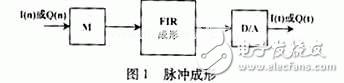
![]()
![]()
![]() That is, the second term in equation (3) is used to represent the sign bit, and the term is not included in the right shift operation of the register, ie it is subtracted from the right shift of the register. Therefore, subtraction control is only used on the sign bit clock throughout the program.
That is, the second term in equation (3) is used to represent the sign bit, and the term is not included in the right shift operation of the register, ie it is subtracted from the right shift of the register. Therefore, subtraction control is only used on the sign bit clock throughout the program. 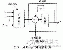


I. Introduction