A manual pulse generator (MPG) is a device normally associated with computer numerically controlled machinery or other devices involved in positioning. It usually consists of a rotating knob that generates electrical pulses that are sent to an equipment controller. The controller will then move the piece of equipment a predetermined distance for each pulse. Manual Pulse Generator,Handwheel MPG CNC,Electric Pulse Generator,Signal Pulse Generator Jilin Lander Intelligent Technology Co., Ltd , https://www.landerintelligent.com
Overview This article compares the differences between DS26303 and IDT82V2048, and specifically explains how to use DS26303 in existing IDT82V2048 applications. The DS26303 is an 8-channel E1 / T1 / J1 short-range line interface unit (LIU) powered by a single 3.3V. No need to change the software to support the IDT82V2048 function, and provide additional features. No need to change the PCB, DS26303 can be used in the existing IDT82V2048 application, only need to change the value of peripheral components according to the application.
The difference in characteristics is divided into three different parts: Table 1 shows some features that DS26303 has but IDT82V2048 does not; Table 2 shows some features that IDT82V2048 has but DS26303 does not. Table 3 shows the common characteristics of DS26303 and IDT82V2048 but different features implemented on the two devices.
Table 6 to Table 10 are the differences between the DS26303 and IDT82V2048 registers and the additional functions provided by the DS26303 additional register set. Figure 1 and Table 11 show the subtle changes that need to be made to the device values ​​when using the DS26303 in existing IDT82V2048 applications.
Table 1. Features of DS26303 different from IDT82V2048 DS26303 IDT82V2048 Programmable opTIon to clear interrupt status on write or read. Clear on read is default. Not supported. Individual channel control for jitter attenuator: Enable / disable FIFO depth FIFO limit trip All channels have global control. Internal software-selectable transmit and receive-side terminaTIon for 100Ω T1 twisted-pair, 110Ω J1 twisted-pair, 120Ω E1 twisted-pair, and 75Ω E1 coaxial applicaTIons. Not supported. In HPS mode, the transmitter output and the internal impedance of the receiver can be turned off with only the OE pin. Requires that both receivers use the same front-end terminaTIon. Built in BERT tester for diagnostics. Not supported. Individual channel control for: Short-circuit protection AIS enable on LOS RCLK inversion TCLK inversion All channels have global control. Individual channel-line violation detection. Not supported. Flexible MCLK See Table 4 for available input frequencies. Not supported. Programmable TECLK output pin (1.544MHz or 2.048MHz) Not supported. Programmable CLKA output pin See Table 5 for available output frequencies. Not supported. Flexible interrupt pin Not supported.
Table 2. Characteristics of IDT82V2048 different from DS26303 DS26303 IDT82V2048 Uses single optimal value. Capability to select the jitter attenuator bandwidth. Not provided. Inband loopack (loopup and loopdown codes). MLCK Pin Functionality
The DS26303 and IDT82V2048 both require MCLK to for data with clock recovery as well as AIS detection.
The MCLK pin of the IDT82V2048 provides additional functionality not present in the DS26303.
IDT82V2048 MCLK held high. The IDT82V2048 slices the incoming bipolar line signal into RZ pulse (data-recovery mode). IDT82V2048 MCLK held low. All the receivers are powered down, and the output pins RCLKn, RDPn, and RDNn are switched to high impedance .Note that wait state generation through RDY / ACK is not available if MCLK is not provided.
Table 3. Differences between DS26303 and IDT82V2048 DS26303 IDT82V2048 3.3V LIU power only, 5V not provided. 5V LIU power. Non-mux Intel® write address to WRB rising-edge setup time is 17ns. Non-mux Intel write address to WRB rising-edge setup time is 6ns. Expects non-mux Intel read address to be valid when RDB is active. Non-mux Intel read address to RDB rising-edge setup time is 6ns. This might be an error in data sheet because data is out before this setup time. Inactive RDY to tri-state delay time 12ns (max). Inactive RDY to tri-state delay time 3ns (max). Clears the interrupt pin when reading or writing the interrupt status. Clear interrupt pin by reading the corresponding status register. Jitter attenuator FIFO depths of 32 bits or 128 bits. Jitter attenuator FIFO depths of 32 bits or 64 bits. Individual channel control for jitter attenuator: Enable / disable FIFO depth FIFO limit trip All channels have global control.
Table 4. DS26303 MCLK selection range PLLE MPS1, MPS0 MCLK MHz (± 50ppm) FREQS T1 or E1 Mode 0 xx 1.544 x T1 0 xx 2.048 x E1 1 00 1.544 1 T1 / J1 or E1 1 01 3.088 1 T1 / J1 or E1 1 10 6.176 1 T1 / J1 or E1 1 11 12.352 1 T1 / J1 or E1 1 00 2.048 0 T1 / J1 or E1 1 01 4.096 0 T1 / J1 or E1 1 10 8.192 0 T1 / J1 or E1 1 11 16.384 0 T1 / J1 or E1
Table 5. DS26303 clock A selection range CLKA3 to CLKA0 MCLK (Hz) 0000 2.048M 0001 4.096M 0010 8.192M 0011 16.384M 0100 1.544M 0101 3.088M 0110 6.176M 0111 12.352M 1000 1.536M 1001 3.072M 1010 6.144M 1011 12.288M 1100 32k 1101 64k 1110 128k 1111 256k
Register considerations DS26303 includes four main register groups. Main register set (DS26303 and IDT82V2048) Secondary register set (DS26303 and IDT82V2048) Independent LIU register set (DS26303 unique) BERT register set (DS26303 unique) In order to take advantage of the additional features and flexibility of the DS26303, the source of the IDT82V2048 application must be Add programs to the code. The address pointer control register (ADDP) has an address of 1Fh, which is used as a pointer to access different register groups. Table 6 shows the DS26303 register set list and the ADDP values ​​required to access these register sets.
Table 6. DS26303 address pointer selection ADDP7 to ADDP0 (Hex) Bank Name DS26303 IDT82V2048 00 Primary Bank Yes Yes AA Secondary Bank Yes Yes 01 Individual LIU Bank Yes No 02 BERT Bank Yes No
The main register set of DS26303 is the same as IDT82V2048. If you use DS26303 to replace the existing IDT82V2048, and only use the main register set, you do not need to modify the application software. Table 7 gives a list of main register banks.
Table 7. Main register set of DS26303 and IDT82V2048 Address (Hex) DS26303 and IDT82V2048 00–15 Primary Registers 16–1E Reserved 1F ADDP
Although both the DS26303 and IDT82V2048 provide secondary register sets, not all registers and their corresponding functions are the same. Table 8 shows the list of registers included in the second-level register set and their functions implemented in the DS26303 and IDT82V2048.
DS26303 contains two other register groups: independent LIU register group and BERT register group. Table 9 is a list of registers included in the independent LIU register set, and Table 10 is a list of registers included in the BERT register set. In order to take advantage of the additional features and flexibility of DS26303, a program must be added to the source code of the IDT82V2048 application.
Table 8. DS26303 secondary register set Address (Hex) Register Name DS26303 IDT82V2048 00 Single-Rail Mode Select Yes Yes 01 Line-Code Selection Yes Yes 02 Clock-Recovery Enable No Yes 03 Receiver Power-Down Enable Yes Yes 04 Transmitter Power-Down Enable Yes Yes 05 Excessive Zero-Detect Enable Yes Yes 06 Code-Violation-Detect Enable Bar Yes Yes 07 Receive Equalizer Enable No Yes 08 Inband Loopback (LB) Configuration No Yes 09 Inband LB Activation Code No Yes 0A Inband LB Deactivation Code No Yes 0B Inband LB Receive Status No Yes 0C Inband LB Interrupt Mask No Yes 0D Inband LB Interrupt Status No Yes 0E Inband LB Activation / Deactivation Code Generator No Yes 1F Set to AAh for access to Secondary Register Bank Yes Yes
Table 9. Independent LIU register set of DS26303 Address (Hex) Register Name 00 Individual JA Enable 01 Individual JA Position Select 02 Individual JA FIFO Depth Select 03 Individual JA FIFO Limit Trip 04 Individual Short-Circuit Protection Disable 05 Individual AIS Select 06 Master-Clock Select 07 Global-Management Register 08–0F Reserved 10 Bit-Error-Rate Tester Control Register 12 Line-Violation Detect Status 13 Receive-Clock Invert 14 Transmit-Clock Invert 15 Clock-Control Register 16 RCLK Disable Upon LOS Register 1E Global-Interrupt Status Control 1F Set to 01h for access to Individual LIU Register Bank
Table 10. BERT register set of DS26303
Hardware considerations You can replace the IDT82V2048 in existing applications with DS26303 without changing the PCB. What needs to be done is to change the external device value according to the target application. Figure 1 shows the recommended network termination circuit for the DS26303, and Table 11 shows the device values ​​required when the DS26303 is properly terminated. Address (Hex) Register Name 00 BERT Control Register 01 Reserved 02 BERT Pattern Configuration 1 03 BERT Pattern Configuration 2 04 BERT Seed / Pattern 1 05 BERT Seed / Pattern 2 06 BERT Seed / Pattern 3 07 BERT Seed / Pattern 4 08 Transmit-Error Insertion Control 09–0A Reserved 0C BERT Status Register 0D Reserved 0E BERT Status Register Latched 10 BERT Status Register Interrupt Enable 11–13 Reserved 14 Receive Bit-Error Count Register 1 15 Receive Bit-Error Count Register 2 16 Receive Bit-Error Count Register 3 17 Receive Bit-Error Count Register 4 18 Receive Bit-Count Register 1 19 Receive Bit-Count Register 2 1A Receive Bit-Count Register 3 1B Receive Bit-Count Register 4 1C–1E Reserved 1F Set to 02h for access to BERT Register Bank
The transmitter IDT82V2048 requires that the transmitter-side resistors be connected in series to the TTIP and TRING outputs. It is recommended that these resistors should be 0Ω (T1 3.3V mode), 9.5Ω (E1 75Ω coaxial) or 9.1Ω (E1 120Ω twisted pair). DS26303 does not require resistance, so the resistance in all modes should be 0Ω.
The receiver is on the receiving side. IDT82V2048 requires a termination impedance of 12.4Ω (T1 3.3V mode), 9.31Ω (E1 75Ω coaxial) or 15Ω (E1 120Ω twisted pair). When using the external impedance mode, the DS26303 requires a 15Ω termination resistor in all cases; when using the DS26303 software to select the impedance matching mode, no resistance is required. IDT82V2048 requires the use of a 1kΩ resistor in series with the RTIP and RRING pins. If the DS26303 uses software to select the termination / impedance matching mode, these 1kΩ resistors can be replaced with 0Ω resistors. 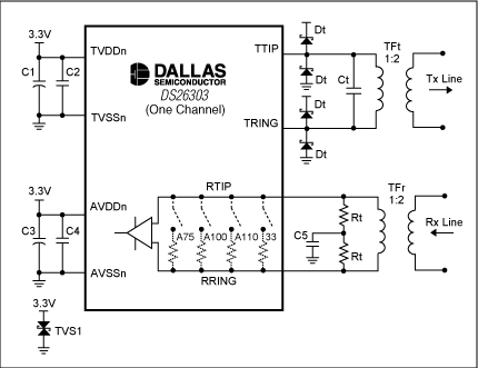
Figure 1. LIU front-end circuit diagram
Table 11. LIU front-end values Mode Component 75Ω Coaxial 120Ω Twisted Pair 100Ω / 110Ω Twisted Pair Tx Capacitance Ct 560pF (typ). Adjust for board parasitics for optimal return loss. Tx Protection Dt International Rectifier: 11DQ04 or 10BQ060 Motorola: MBR0540T1 Rx Transformer 1: 2 TFr Pulse: T1124 (0 ° C to + 70 ° C) Tx Transformer 1: 2 TFt Pulse: T1114 (-40 ° C to + 85 ° C) Tx Decoupling (ATVDD) C1 Common decoupling for all eight channels is 68µF. Tx Decoupling (ATVDD) C2 Recommended decoupling per channel is 0.1µF. Rx Decoupling (AVDDn) C3 Common decoupling for all eight channels is 68µF. Rx Decoupling (AVDDn) C4 Common decoupling for all eight channels is 0.1µF. Rx Termination C5 When in external impedance mode, Rx capacitance for all eight channels is 0.1µF. Do not populate if using internal impedance mode. Rx Termination Rt When in external impedance mode, the two resistors for all modes shall be 15.0Ω ± 1%. Do not populate if using internal impedance mode. Voltage Protection TVS1 SGS-Thomson: SMLVT 3V3 (3.3V transient suppressor)
The CNC handheld controller MPG Pendant with x1, x10, x100 selectable. It is equipped with our popular machined MPG unit, 4,5,6 axis and scale selector, emergency stop and reset button.
Abstract: This article compares the differences between DS26303 and IDT82V2048, specifically explains how to use DS26303 in existing IDT82V2048 applications, and elaborate on the differences in their characteristics, considerations in register and hardware design.