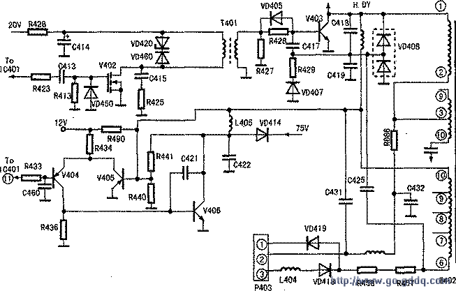
The simplified circuit diagram of the TPV S569P color display line output is shown in the figure (the dotted line indicates that the components in the circuit are not drawn). The excitation circuit of the machine adopts a reverse polarity excitation mode, that is, when the row excitation tube V402 is turned on, the output tube V403 is turned off, and during V402, the V403 is turned on. Because the machine is a multi-frequency scanning display, in order to prevent the power consumption of V403 from increasing at different frequencies, the V402 uses a FET with good shutdown performance. The row excitation transformer T401 provides the V403 with a switching pulse current that operates in a switching state. Excessive current can cause the V403be junction to blow. Therefore, a current limiting resistor R428 and a shunt resistor R427 are connected in series on the b pole of V403. At the same time, the R427 also forms a bleeder circuit with the VD405. During V402 turn-on, the lower positive and negative pulse voltage induced on the secondary winding of T401 is discharged through 1t427 and VD405 to prevent excessive reverse current from causing breakdown of V403be junction. C415 and R425 constitute a damping circuit to prevent damage during the V402 cut-off period due to excessive D-peak voltage. During V403 saturation conduction, the B+ voltage is supplemented with magnetic energy by T402 in the primary winding (1~2 winding) of the output transformer T402, and the original stored energy of the S correction capacitor C425 is passed through the T402 primary winding and the row deflection coil H. The DY and the output of the line output tube V403 are grounded to ground. at this time. The magnetic field generated in H.DY controls the electron beam to complete the scanning from the center of the grating to the right half. During the V403 cut-off period, the current in H.DY cannot be abruptly changed, so that the induced electromotive force is generated in H.DY, and the line-reverse capacitors C418 and C419 are charged. When the charging current drops to 0, the voltage across C418 and C419 reaches its maximum. The voltage across C418 and C419 is then gradually reduced to 0 by H.DY discharge, completing the whole process of reverse retrace. Until the current in H.DY reaches the reverse maximum. All electrical energy is converted into magnetic energy. At this time, the double damper tube VD408 composed of two Schottky diodes is positively biased. The current in H.DY forms a loop through VD408, which controls the electron beam to complete the scanning from the center of the grating to the left half.
Focusing on the development and production of Wireless Charging products that make life easier.
Supply various wireless charger including multifunctional Wireless Charger, Car Wireless Charger, Magnetic Wireless Chargin, Wireless Charging Mouse Pad, etc.
We help 200+ customers create custom wireless charging products design for various industries.
Manufacturing high quality products for customers according to international standards, such as CE ROHS FCC REACH UL SGS BQB etc.
Wireless Charging Pad,Wireless Phone Charger,Wireless Car Charger,Bluetooth Charger TOPNOTCH INTERNATIONAL GROUP LIMITED , https://www.micbluetooth.com